Fairchild Semiconductor FST3253QSCX, FST3253QSC, FST3253MX, FST3253MTCX, FST3253MTC Datasheet
...
© 1999 Fairchild Semiconductor Corporation DS500058 www.fairchildsemi.com
September 1997
Revised December 1999
FST3253 Dual 4:1 Multiplexer/Demultiplexer Bus Switch
FST3253
Dual 4:1 Multiplexer/Demultiplexer Bus Switch
General Description
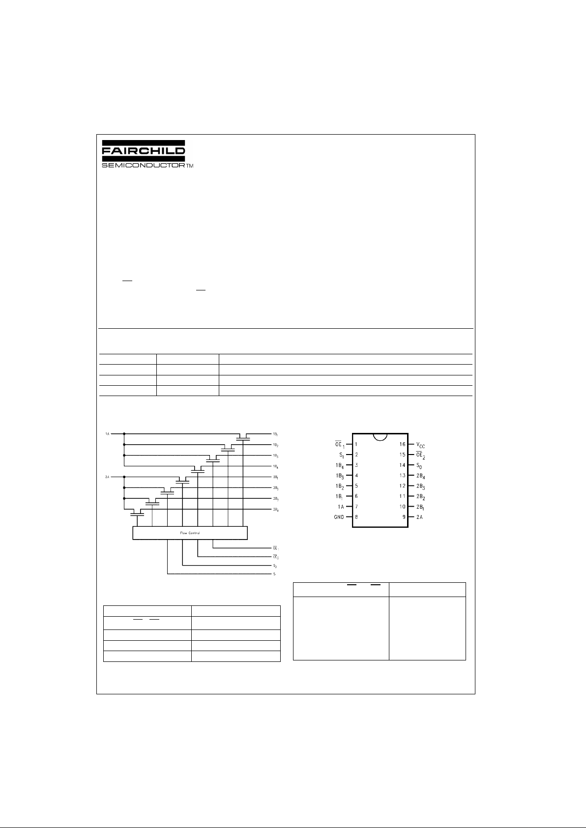
The Fairchild Switch FST3253 is a dual 4:1 high-speed
CMOS TTL-compatible multiplexer/demultiplexer bus
switch. The low on resistance of the switch allows inputs to
be connected to outputs wi thout a dding pr opagation delay
or generating additional ground bounce noise.
When OE
is LOW, S0 and S1 connect the A Port to the
selected B Port output. When OE
is HIGH, the switch is
OPEN and a high-impedance sta te exist s between the two
ports.
Features
■ 4Ω switch connection between two ports.
■ Minimal propagation delay through the switch.
■ Low l
CC
.
■ Zero bounce in flow-through mode.
■ Control inputs compatible with TTL level.
Ordering Code:
Device also available in Tape and Reel. Specify by appending s uffix let te r “X” to the ordering code.
Logic Diagram
Pin Descriptions
Connection Diagram
Truth Table
Order Number Package Number Package Description
FST3253M M16A 16-Lead Small Outline Integrated Circuit (SOIC), JEDEC MS-012, 0.150 Narrow
FST3253QSC MQA16 16-Lead Quarter Size Outline Package (QSOP), JEDEC MO-137, 0.150 Wide
FST3253MTC MTC16 16-Lead Thin Shrink Small Outline Package (TSSOP), JEDEC MO-153, 4.4mm Wide
Pin Name Description
OE
1
, OE
2
Bus Switch Enables
S
0
, S
1
Select Inputs
ABus A
B
1
, B2, B3, B
4
Bus B
S1S0OE1OE
2
Function
X X H X Disconnect 1A
X X X H Disconnect 2A
LLLL A = B
1
LHLL A = B
2
HLLL A = B
3
HHL L A = B
4

www.fairchildsemi.com 2
FST3253
Absolute Maximum Ratings(Note 1) Recommended Operating
Conditions
(Note 3)
Note 1: The Absolute Maximum Ratings are those values beyond which
the safety of the dev ice cannot be guaranteed. T he device sh ould not be
operated at these limit s. The parametric values defin ed in the Electrical
Characteristics tables are not guaranteed at the absolute maximum rating.
The Recommende d Opera ting Condit ions table s will de fine the co nditions
for actual device operation.
Note 2: The input and output ne gative vo ltage ra tings may be excee ded if
the input and output diode current ratings are observed.
Note 3: Unused control inputs must be held HIGH or LOW. They may not
float.
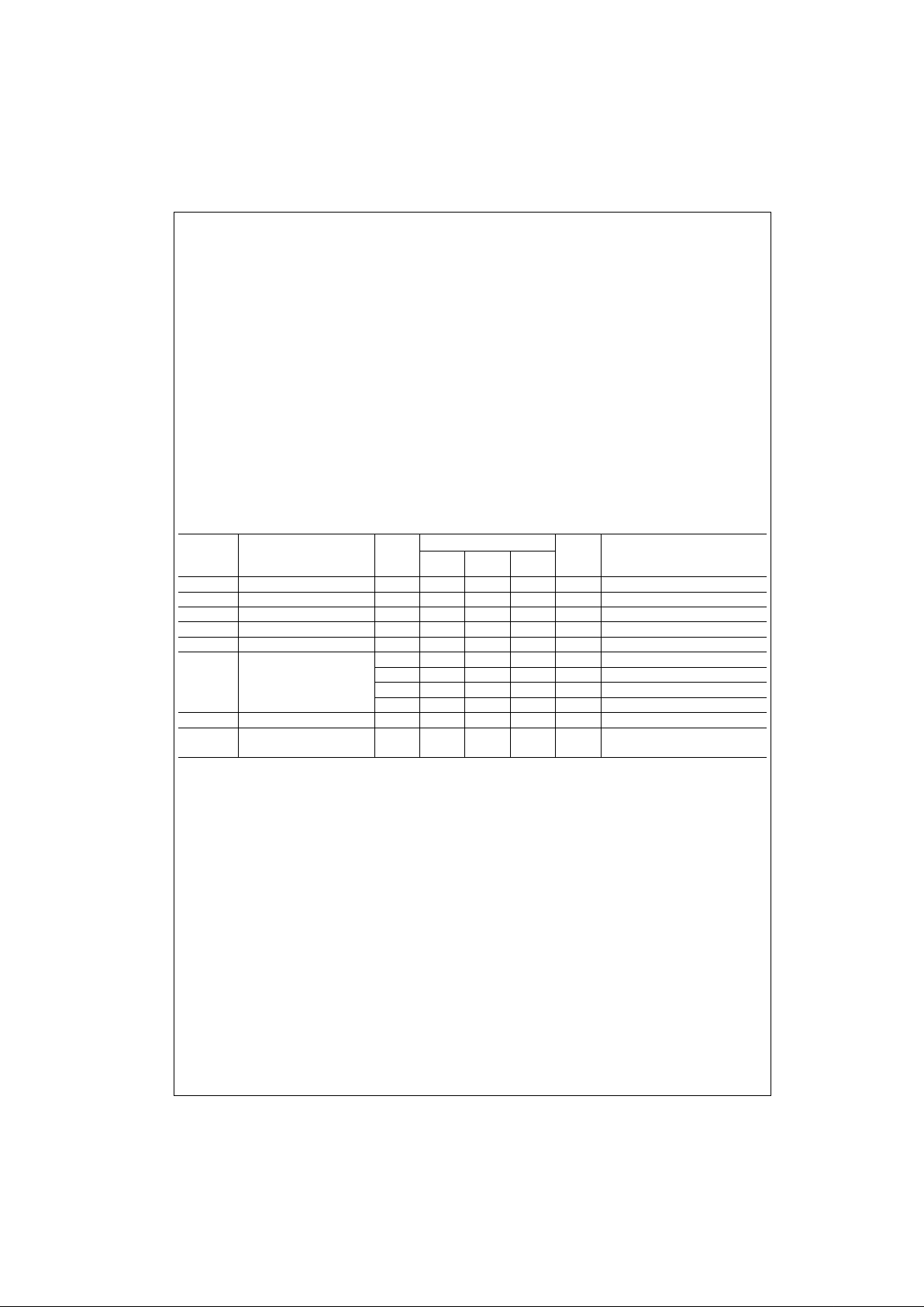
DC Electrical Characteristics
Note 4: Typi c al values are at VCC = 5.0V and TA = +25°C
Note 5: Measured by the volta ge drop between A and B pi ns at th e indicated current through the switch. On resistance is determined by the lower of the
voltages on the two (A or B) pins.
Supply Voltage (VCC) −0.5V to +7.0V
DC Switch Voltage (V
S
) −0.5V to +7.0V
DC Input Voltage (V
IN
)(Note 2) −0.5V to +7.0V
DC Input Diode Current (l
IK
) VIN<0V −50mA
DC Output (I
OUT
) Sink Current 128mA
DC V
CC
/GND Current (ICC/I
GND
) +/− 100mA
Storage Temperature Range (T
STG
) −65°C to +150 °C
Power Supply Operating (V
CC)
4.0V to 5.5V
Input Voltage (V
IN
)0V to 5.5V
Output Voltage (V
OUT
)0V to 5.5V
Input Rise and Fall Time (t
r
, tf)
Switch Control Input 0ns/V to 5ns/V
Switch I/O 0ns/V to DC
Free Air Operating Temperature (T
A
) −40 °C to −85 °C
Symbol Parameter
V
CC
(V)
T
A
= −40 °C to +85 °C
Units Conditions
Min
Typ
(Note 4)
Max
V
IK
Clamp Diode Voltage 4.5 −1.2 V IIN = −18mA
V
IH
High Level Input Voltage 4.0–5.5 2.0 V
V
IL
Low Level Input Voltage 4.0–5.5 0.8 V
I
I
Input Leakage Current 5.5 ±1.0 µA0≤ VIN ≤5.5V
I
OZ
OFF-STATE Leakage Current 5.5 ±1.0 µA0 ≤A, B ≤V
CC
R
ON
Switch On Resistance 4.5 4 7 Ω VIN = 0V, IIN = 64mA
(Note 5) 4.5 4 7 Ω V
IN
= 0V, IIN = 30mA
4.5 8 15 Ω V
IN
= 2.4V, IIN = 15mA
4.0 11 20 Ω VIN = 2.4V, IIN = 15mA
I
CC
Quiescent Supply Current 5.5 3 µAVIN = VCC or GND, I
OUT
= 0
∆ I
CC
Increase in I
CC
per Input 5.5 2.5 mA One input at 3.4V
Other inputs at VCC or GND
 Loading...