

Fairchild Semiconductor FST16232MTDX, FST16232MTD, FST16232MEAX, FST16232MEA, FST16232CW Datasheet
© 1999 Fairchild Semiconductor Corporation DS500054 www.fairchildsemi.com
July 1997
Revised December 1999
FST16232 Synchronous 16-Bit to 32-Bit Multiplexer/Demultiplexer Bus Switch
FST16232
Synchronous 16-Bit to 32-Bit
Multiplexer/Demultiplexer Bus Switch
General Description
The Fairchild Swi tch FST16232 is a 1 6-bit to 32-bit hig hspeed CMOS TTL-compatible synchronous multiplexer/
demultiplexer bus switch. The low on resistance of the
switch allows inputs to be connected to outputs without
adding propagation de lay or generating addition al ground
bounce noise.
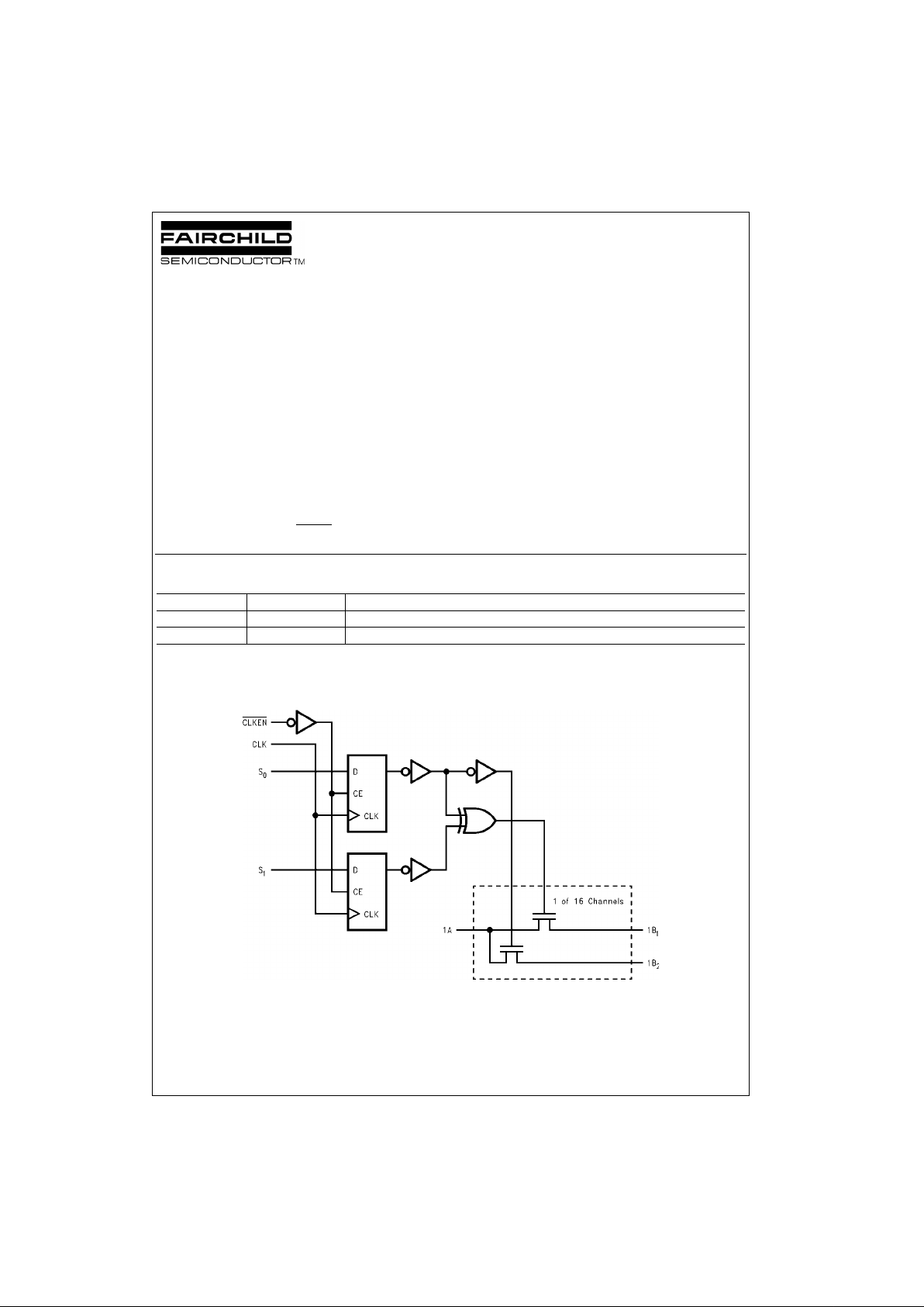
The device allows two separate datapaths to be multiplexed onto, or demultiplexed from, a single path. Two control select pins (S
1
, S0) are synchronous and clocke d on
the rising edge of CLK when CLKEN
is LOW.
Features
■ 4Ω switch connection between two ports.
■ Minimal propagation delay through the switch.
■ Low l
CC
.
■ Zero bounce in flow-through mode.
■ Control inputs compatible with TTL level.
Ordering Code:
Devices also availab le in Tape and Reel. Specify by appending th e s uffix let t er “X” to the ordering code.
Logic Diagram
Order Number Package Number Package Description
FST16232MEA MS56A 56-Lead Shrink Small Outline Package (SSOP), JEDEC MO-118, 0.300 Wide
FST16232MTD MTD56 56-Lead Thin Shrink Small Outline Package (TSSOP), JEDEC MO-153, 6.1mm Wide

www.fairchildsemi.com 2
FST16232
Connection Diagram Pin Descriptions
Tr uth Table
Pin Name Description
S
1
, S
0
Control Pins
CLK Clock Input
CLKEN
Clock Enabl e Input
1A, 2A Bus A
1B, 2B Bus B
Inputs
Function
S
1S0
CLK CLKEN
X X X H Last State
LL ↑ L Disconnect
LH ↑ LA = B
1
and A = B
2
HL ↑ LA = B
1
HH ↑ LA = B
2
 Loading...