Fairchild Semiconductor FSLV16211 Datasheet

FSLV16211
24-Bit Bus Switch
FSLV16211 24-Bit Bus Switch
February 2001
Revised March 2003
General Description
The FSLV16211 is a 24-bit, high speed, low v oltage bus
switch. The low On Resistance of t he switch allows inputs
to be connected to outputs without adding propagation
delay or generating additional ground bounce noise.
This device’s design al low this part to be used a s a 12-bit
or 24-bit bus switch. When OE
nected to Port 1B. When OE
to Port 2B.
is LOW, Port 1A is con-
1
is LOW, Port 2A is connected
2
Features
■ 5Ω switch connection between two ports
■ Minimal propagation delay through the switch
■ Low l
CC
■ Zero bounce in flow-through mode
■ Also packaged in plastic Fine-Pitch Ball Grid Array
(FBGA)
Ordering Code:
Order Number Package Number Package Description
FSLV16211G
(Note 1)(Note 2)
FSLV16211MTD
(Note 2)
Note 1: Ordering code “G” indicates Trays.
Note 2: Devices also available in Tape and Reel. Specify by appending th e s uffix let t er “X” to the ordering code.
BGA54A 54-Ball Fine-Pitch Ball Grid Array (FBGA), JEDEC MO-205, 5.5mm Wide
MTD56 56-Lead Thin Shrink Small Outline Package (TSSOP), JEDEC MO-153, 6.1mm Wide
Logic Diagram
© 2003 Fairchild Semiconductor Corporation DS500451 www.fairchildsemi.com

Connection Diagrams
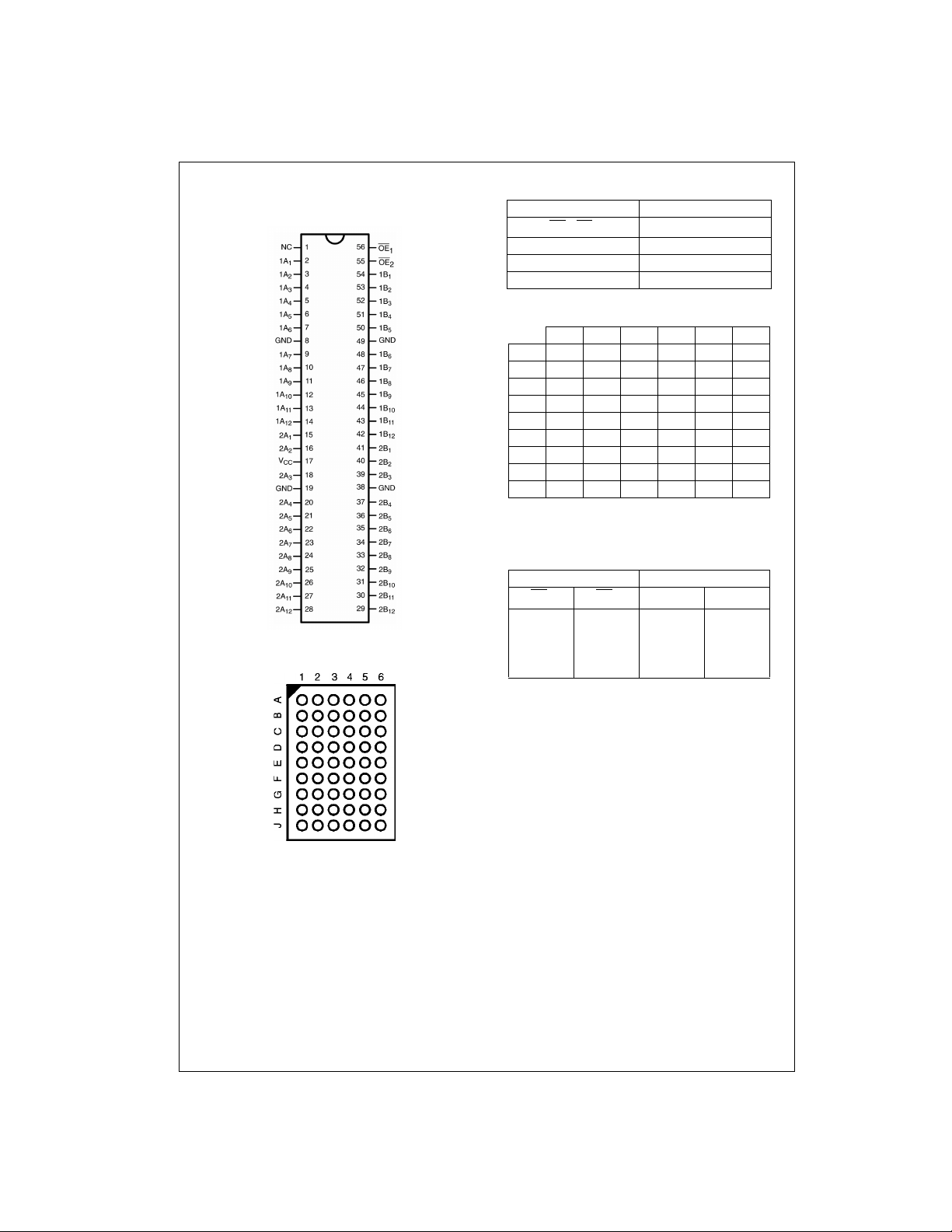
Pin Assignment for TSSOP
FSLV16211
Pin Assignment for FBGA
Pin Descriptions
Pin Name Description
OE
1
, OE
2
Bus Switch Enables
1A, 2A Bus A
1B, 2B Bus B
NC No Connect
FBGA Pin Assignments
123456
A 1A
1A1NC OE21B11B
2
B 1A41A31A7OE11B31B
C 1A61A5GND 1B71B51B
D 1A101A91A81B81B91B
E 1A121A112A12B11B111B
F 2A42A32A22B22B32B
G 2A62A5VCCGND 2B52B
H 2A82A72A92B92B72B
J 2A122A112A102B102B112B
Truth Table
Inputs Inputs/Outputs
OE
1
LL1A
LH1A
HLZ2A
HHZZ
OE
1A, 1B 2A, 2B
2
= 1B 2A = 2B
= 1B Z
2
4
6
10
12
4
6
8
12
= 2B
(Top Thru View)
www.fairchildsemi.com 2
 Loading...