

Fairchild Semiconductor FS6S1565RB Datasheet
FS6S1565RB
Fairchild Power Switch(FPS)
www.fairchildsemi.com
Features
• Wide operating frequency range up to 150Khz
• Internal Burst mode Controller for Stand-by mode
• Pulse by pulse over current limiting
• Over current protection(Auto restart mode)
• Over voltage protection (Auto restart mode)
• Over load protection(Auto restart mode)
• Internal thermal shutdown function(Auto restart mode)
• Under voltage lockout
• Internal high voltage sense FET
• Eternal sync terminal/Soft start
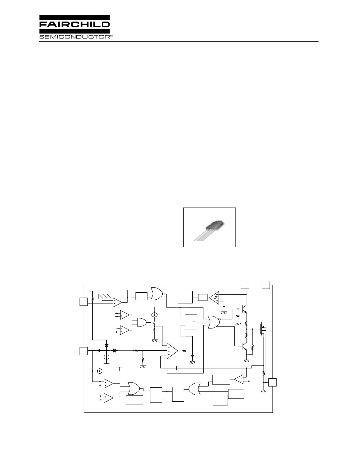
Internal Block Diagram
Description
The Fairchild Power Switch(FPS) product family is specially
designed for an off-line SMPS with minimal external
components. The Fairchild Power Switch(FPS) consist of
high voltage power SenseFET and current mode PWM IC.
Included PWM controller features integrated fixed oscillator,
under voltage lock out, optimized gate turn-on/turn-off
driver, thermal shut down protection, over voltage protection,
and temperature compensated precision current sources for
loop compensation and fault protection circuitry . compared to
discrete MOSFET and controller or R
converter solution, a Fairchild Power Switch(FPS) can
reduce total component count, design size, and weight and at
the same time increase efficiency, productivity, and system
reliability. It has a basic platform well suited for cost
effective monitor power supply.
TO-3P-5L
1
switching
CC
Vref
Vpp=5.8/7.2V
Vfb
Vth=1V
Vcc
Vth=11V/12V
5555
4444
Ifb
Vref
Vcc
Idelay
OLP
Vth=7.5V
Vcc
Vth=30V
©2001 Fairchild Semiconductor Corporation
OVP
Burst mode
controller
2.5R
R
UVLO Reset
(Vcc=9V)
OSC
Vref
S
R
11113333
UVLO
Filter
(130nsec)
UVLO Reset
(Vcc=9V)
Ron
Roff
Rsenese
TS
D
(Tj=160℃
Vth=1V
)
2222
Internal
PWM
Vfb Offset
S
Q
Q
R
Bias
S
R
Vref
Q
OCL
Rev.1.0.1

FS6S1565RB
Absolute Maximum Ratings
(Ta=25°C, unless otherwise specified)
Parameter Symbol Value Unit
Drain-source(GND) voltage
Drain-Gate Voltage (R
Gate-source (GND) Voltage V
Drain current pulsed
Single pulsed avalanche energy
Single Pulsed Avalanche current
Continuous drain current (Tc = 25°C) I
Continuous drain current (TC=100°C) I
Supply voltage V
Input Voltage Range
Total Power Dissipation
Operating junction temperature T
Operating Ambient Temperature T
Storage Temperature range T
(1)
=1MΩ)V
GS
(2)
(3)
(4)
V
DSS
DGR
GS
I
DM
E
AS
I
AS
D
D
CC
V
FB
V
S_S
(Watt H/S) 270 W
P
D
Derating 2.17 W/°C
j
A
STG
650 V
650 V
±30 V
60 A
1040 mJ
37 A
15 A
9.5 A
35 V
−0.3 to V
CC
−0.3 to 10 V
+160 °C
−25 to +85 °C
−55 to +150 °C
DC
DC
DC
V
Notes:
1. Tj=25°C to 150°C
2. Repetitive rating: Pulse width limited by maximum junction temperature
3. L=8.5mH, starting Tj=25°C
4. L=13uH, starting Tj=25°C
2

Electrical Characteristics (SFET part)
(Ta=25°C unless otherwise specified)
Parameter Symbol Condition Min. Typ. Max. Unit
Drain-source breakdown voltage BV
Zero gate voltage drain current I
Static drain-source on resistance
Forward transconductance
(note)
(note)
DSS
DSS
R
DS(ON)
gfs V
Input capacitance Ciss
Reverse transfer capacitance Crss - 50 Turn on delay time t
d(on)
Rise time tr - 155 Turn off delay time t
d(off)
Fall time tf - 125 Total gate charge
(gate-source+gate-drain)
Qg
Gate source charge Qgs - 15 Gate drain (Miller) charge Qgd - 45 -
Single Pulsed Avalanche current
Note:
Pulse test : Pulse width ≤ 300µS, duty 2%
1
S
--- -=
R
1. L=13uH, starting Tj=25°C
(1)
I
AS
V
= 0V, ID = 250µA 650 - - V
GS
V
= 650V, V
DS
V
= 520V
DS
V
= 0V, TC = 125°C
GS
V
= 10V, ID = 7.5A - 0.5 0.65
GS
= 50V, ID = 7.5A - - - S
DS
= 0V - - 200 µA
GS
- - 300 µA
- 2580 -
V
GS
= 0V, V
DS
= 25V,
f = 1MHz
V
= 325V, ID = 15A
DD
-50(MOSFET switching
time are essentially
independent of
- 270 operating temperature)
V
= 10V, ID = 15A,
GS
V
= 520V (MOSFET
DS
-90Switching time are
Essentially independent of
Operating temperature)
V
= V
= V
CC
FB
= GND - 37 - A
SS
FS6S1565RB
Ω
pFOutput capacitance Coss - 270 -
nS
nC
3

FS6S1565RB
Electrical Characteristics
(Ta=25°C unless otherwise specified)
Parameter Symbol Condition Min. Typ. Max. Unit
UVLO SECTION
Start threshold voltage V
Stop threshold voltage V
START
STOP
SENSEFET SECTION
Drain to PKG Breakdown voltage BVpkg 60HZ AC, Ta = 25°C 3500 - - V
Drain to Source Breakdown voltage BVdss Vdrain = 650V, Ta = 25°C 650 - - V
Drain to Source Leakage current Idss Vdrain = 650V, Ta = 25°C - - 300 uA
OSCILLATOR SECTION
Initial Frequency F
Voltage Stability F
Temperature Stability (note4) ∆F
Maximum duty cycle D
Minimum Duty Cycle D
OSC
STABLE
OSC
MAX
MIN
FEEDBACK SECTION
Feedback source current I
Shutdown Feedback voltage V
FB
SD
Shutdown delay current Idelay V
PROTECTION SECTION
Over Voltage Protection V
Over Current Latch Voltage (Note2) V
Thermal Shutdown Temp.(Note4) T
OVP
OCL
SD
V
= GND 14 15 16 V
FB
V
= GND 8910V
FB
-222528kHz
12V ≤ Vcc ≤ 23V 0 1 3 %
-25°C ≤ Ta ≤ 85°C0±5±10%
-929598%
---0%
V
= GND 0.7 0.9 1.1 mA
FB
Vfb ≥ 6.9V 6.9 7.5 8.1 V
= 5V 1.6 2.0 2.4 µA
FB
Vsync ≥ 11V 27 30 33 V
-0.91.01.1V
- 140 160 - °C
4
 Loading...