

Fairchild Semiconductor FS6S1265RE Datasheet
FS6S1265RE
Fairchi ld Pow er Sw itch( FP S)
www.fairchildsemi.com
Features
• Wide Operating Frequency Rang e Up to 150kHz
• Lowest Cost SMPS Solution
• Lowest External Components
• Low Start up Current (Max:170uA)
• Low Operating Current (Max:15mA)
• Internal High Voltage SenseFET
• Built-in Auto Restart Circuit
• Over Voltage Protection (Auto Restart Mode)
• Over Load Protection (Auto Restart Mode)
• Over Current Protection (Auto Restart Mode)
• Internal Thermal Protection (Auto Restart Mode)
• Pulse By Pulse Over Current Limiting
• Internal Burst Mode Controller for Stand-by Mode
• Under Voltage Lockout With Hysteresis
• External Sync. Terminal
Description
The Fairchild Power Switch(FPS) product family is specially
designed for an off line SMPS with minimal external
components. The Fairchild Power Switch(FPS) consist of
high voltage power SenseFET and current mode PWM IC.
Included PWM controller features integrated fixed oscillator,
under voltage lock out, optimized gate turn on/turn off driver,
thermal shut down protection, over voltage protection, and
temperature compensated precision current sources for loop
compensation and fault protection circuitry . compared to
discrete MOSFET and controller or R
solution, a Fairchild Power Switch(FPS) can reduce total
component count, design size, and weight and at the same
time increase efficiency, productivity, and system reliability.
It has a basic platform well suited for cost effective monitor
power supply.
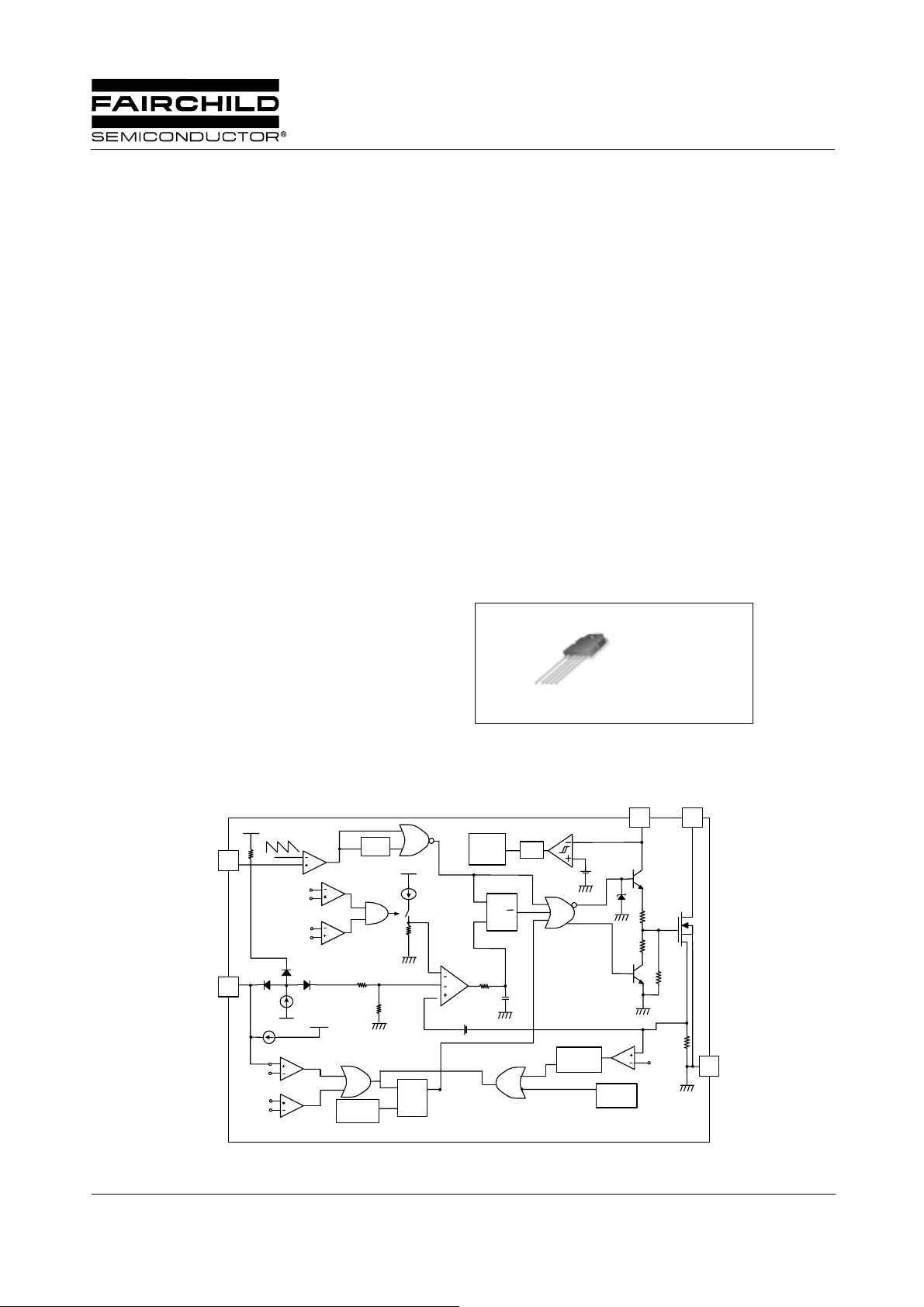
TO-3P-5L
1
1. Drain 2. Gnd 3. V
4. FeedBack 5. Sync.
CC
switching converter
CC
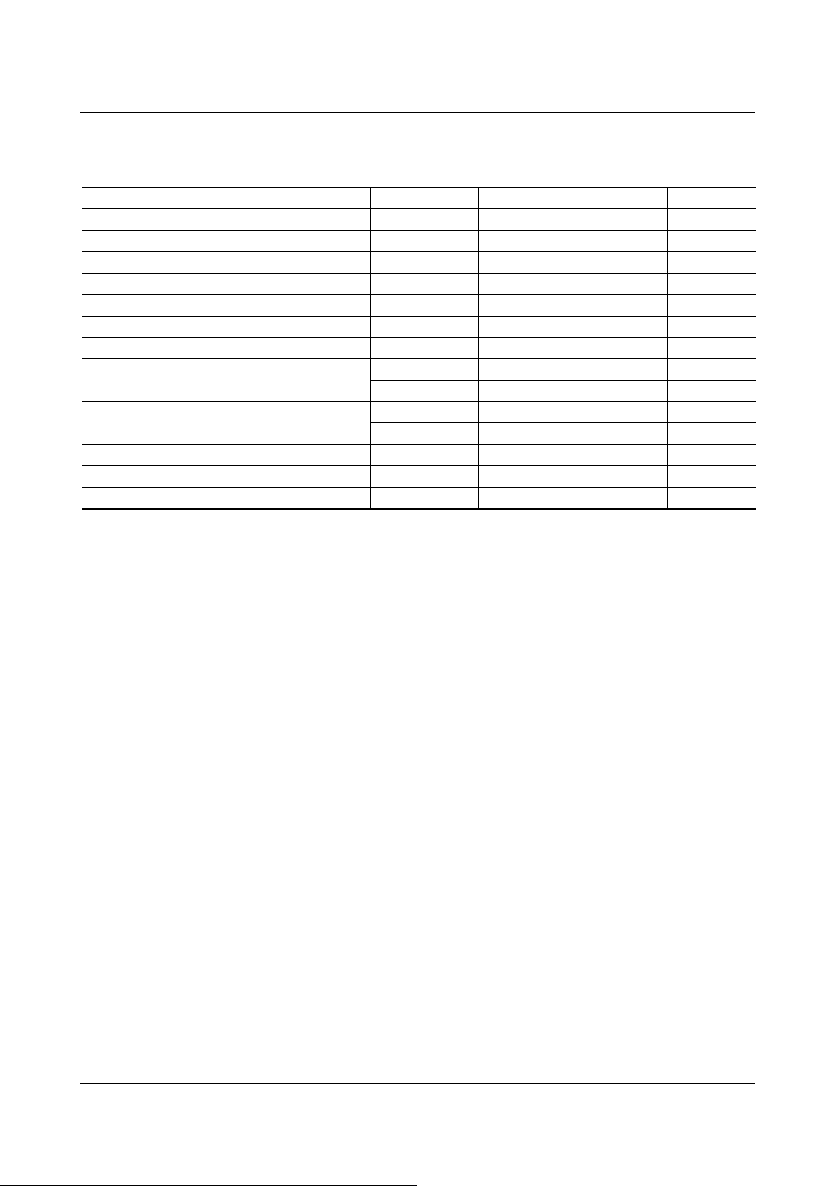
Internal Block Diagram
Vref
Vpp=5.8/7.2V
Vfb
Vth=1V
Vcc
Vth=11V/12V
Vref
Idelay
Ifb
OLP
OVP
SoftStart
SoftStart
SoftStart SoftStart
& Sync
& Sync
& Sync& Sync
Feedback
Feedback
FeedbackFeedback
5555
4444
Vth=7.5V
Vcc
Vth=30V
©2003 Fairchild Semiconductor Corporation
Vcc
Burst mode
controller
2.5R
R
UVLO Reset
(Vcc=9V)
OSC
Vref
S
R
Drain
Drain
Ron
Vth=1V
Rsenese
DrainDrain
11113333
GND
GND
GNDGND
2222
Vcc
Vcc
VccVcc
OCL
UVLO
(130nsec)
Filter
TS
D
(Tj=160℃
Roff
)
Internal
PWM
Vfb Offset
Q
Bias
S
R
Vref
Q
Rev.1.0.1
FS6S1265RE
Absolute Maximum Ratings
(Ta=25°C, unless otherwise specified)
Characteristic Symbol Value Unit
Drain-Gate Voltage(R
=1MΩ) V
GS
Gate-Source(GND) Voltage V
Drain Current Pulsed
(1)
I
Continuous Drain Current (Tc = 25°C) I
Continuous Drain Current (Tc = 100°C) I
(3)
Single Pulsed Avalanche Current
(Energy
Maximum Supply Voltage V
Input Voltage Range
Total Power Dissipation
(2)
)IAS(EAS) 30(950) A(mJ)
CC,MAX
V
V
D
(Watt H/S) 240 W
P
Darting 1.92 W/°C
Operating Junction Temperature. T
Operating Ambient Temperature. T
Storage Temperature Range. T
DGR
GS
DM
D
D
FB
SS
J
A
STG
650 V
±30 V
48 ADC
12 ADC
8.4 ADC
35 V
-0.3 to V
CC
-0.3 to 10 V
+150 °C
-25 to +85 °C
-55 to +150 °C
V
Note:
1. Repetitive rating: pulse width limited by maximum junction temperature
2. L = 10mH, starting T
3. L = 13uH, starting Tj = 25
= 25
j
°C
°C
2
FS6S1265RE
Electrical Characteristics (SFET Part)
(Ta = 25°C unless otherwise specified)
Parameter Symbol Conditions Min. Typ. Max. Unit
V
Drain-Source Breakdown Voltage BV
Zero Gate Voltage Drain Current I
Static Drain-Source on Resistance
Forward Transconductance
(2)
(1)
DSS
DSS
R
DS(on)
gfs V
Input Capacitance Ciss
Output Capacitance Coss - 185 Reverse Transfer Capacitance Crss - 32 Turn on Delay Time t
d(on)
Rise Time tr - 120 Turn Off Delay Time t
d(off)
Fall Time tf - 100 Total Gate Charge
(Gate-Source+Gate-Drain)
Qg
Gate-Source Charge Qgs - 10 -
Gate-Drain (Miller) Charge Qgd - 30 -
= 0V, ID = 50µA 650 - - V
GS
VDS=Max, Rating, V
= 0.8Max, Rating,
V
DS
V
= 0V, TC = 125°C
GS
V
= 10V, ID = 4.5A - 0.7 0.9 Ω
GS
DS
= 50V, ID = 4.5A - - - S
= 0V - - 200 µA
GS
- - 300 µA
- 1820 -
GS
V
= 0V, V
DS
= 25V,
f = 1MHz
V
DD
= 0.5BV
DSS
, ID = 12.0A
-38(MOSFET switching
time are essentially
independent of
- 200 operating temperature)
GS
= 10V, ID = 12.0A,
V
V
DS
= 0.5BV
DSS
(MOSFET
-60Switching time are
Essentially independent of
Operating temperature)
pF
nS
nC
Note:
1. Pulse test: pulse width ≤ 300us, duty 2%
1
S
--- -=
2.
R
3
 Loading...