

Fairchild Semiconductor FS6M07652RTC Datasheet
FS6M07652RTC
Fairchi ld Pow er Sw itch( FP S)
www.fairchildsemi.com
Features
• Fixed Frequency
• Internal Burst Mode Control ler for Stand-by Mode
• Pulse By Pulse Over Current Limiting
• Over Current Protection(Auto Restart Mode)
• Over Voltage Protection (Auto Restart Mode)
• Over Load Protection(Auto Restart Mode)
• Internal Thermal Shutdown Function(Latch Mode)
• Under Voltage Lockou t
• Internal High Voltage Sense FET
•Soft Start
Application
• LCD Monitor SMPS
• Adaptor
Description
The Fairchild Power Switch(FPS) product family is specially
designed for an off line SMPS with minimal external
components. The Fairchild Power Switch(FPS) consist of a
high voltage power SenseFET and a current mode PWM IC.
Included PWM controller features integrated fixed oscillator,
the under voltage lock out, the leading edge blanking, the
optimized gate turn-on/turn-off driver, the thermal shutdown
protection, the over voltage protection, and the temperature
compensated precision current sources for the loop
compensation and a fault protection circuitry. compared with
a discrete MOSFET and a controller or a RCC switching
converter solution, a Fairchild Power Switch(FPS) can
reduce total component count, design size, and weight and at
the same time increase efficiency, productivity, and system
reliability. It has a basic platform well suited for the cost
effective LCD monitor power supply.
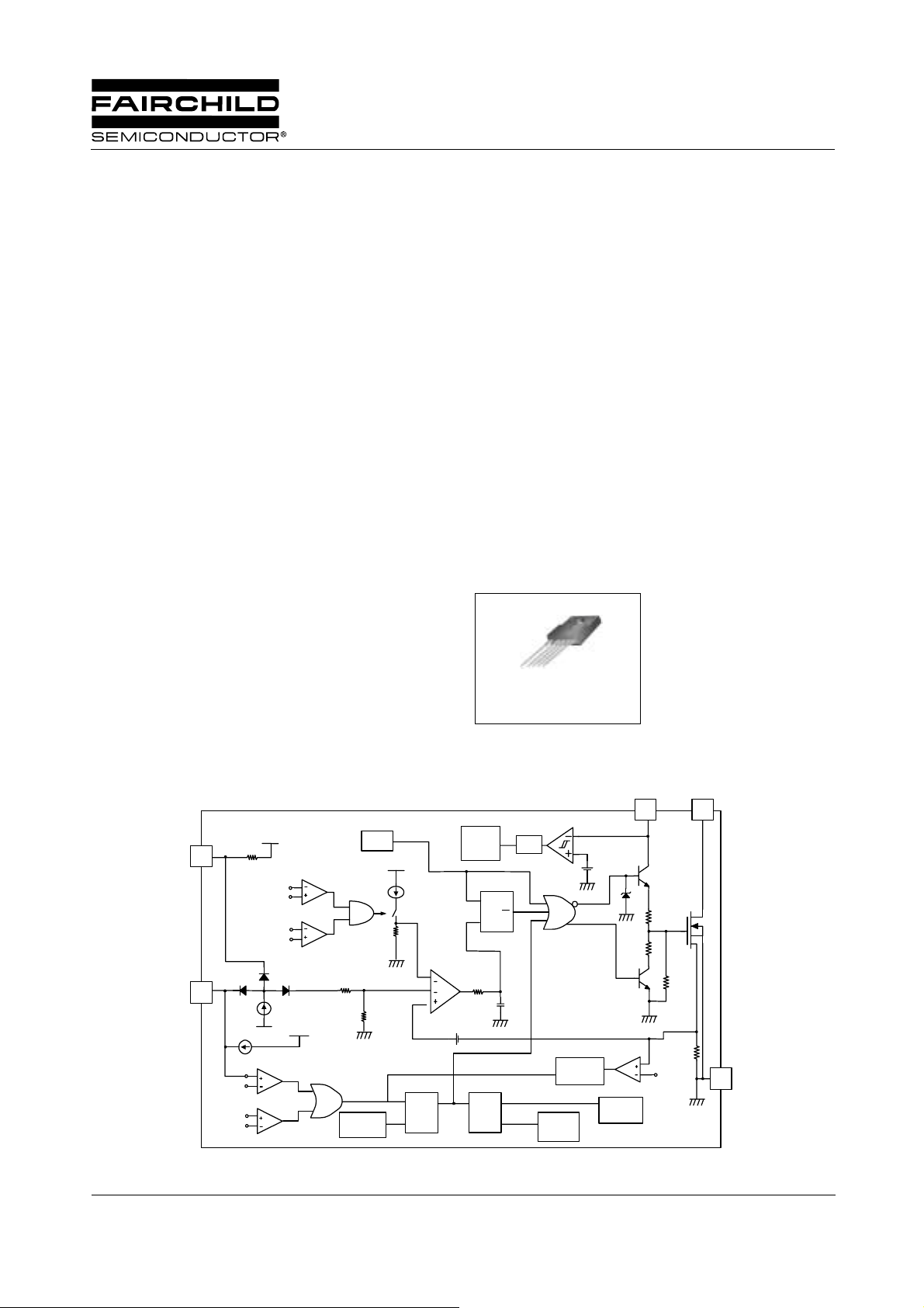
TO-220F-5L
1
1. Drain 2. GND 3. V
4. Feedback 5. SoftStart
CC
Internal Block Diagram
Vref
SoftStart
Feedbock
5555
4444
Vth=7.5V
Vcc
Vth=33V
Vth=1V
Vth=11V/12V
Vref
Idelay
Vfb
Vcc
Ifb
Vcc
OLP
OVP
V
CC
Vfb Offset
Q
PWM
Internal
Bias
Q
S
R
S
R
Vref
Q
OCL
OSC
Vref
Burst mode
controller
2.5R
R
UVLO Reset
(Vcc=9V)
S
R
UVLO
(130nsec)
Power-on
Reset
(Vcc=6.5V)
Filter
Roff
TSD
(Tj=160℃
)
Ron
Vth=2V
Rsenese
Drain
11113333
GND
2222
Rev.1.0.4
©2003 Fairchild Semiconductor Corporation

FS6M07652RTC
Absolute Maximum Ratings
(Ta=25°C, unless otherwise specified)
Characteristic Symbol Value Unit
Drain-Gate Voltage (R
=1MΩ)V
GS
DGR
Gate-Source (GND) Voltage V
Drain Current Pulsed
(1)
I
Continuous Drain Current (Tc = 25°C) I
Continuous Drain Current (TC=100°C) I
Single Pulsed Avalanche Current
(3)
(Energy
Maximum Supply Voltage V
Input Voltage Range
Total Power Dissipation
(2)
)I
AS(EAS
CC, MAX
V
V
(Watt H/S) 46 W
P
D
Darting 0.37 W/°C
Operating Junction Temperature T
Operating Ambient Temperature T
Storage Temperature Range T
STG
GS
DM
D
D
) 17(570) A(mJ)
FB
SS
j
A
650 V
±30 V
14.4 A
3.6 A
2.28 A
35 V
-0.3 to V
CC
-0.3 to 10 V
+150 °C
-25 to +85 °C
-55 to +150 °C
DC
DC
DC
V
Notes:
1. Repetitive rating: Pulse width limited by maximum junction temperature
2. L=81mH, starting Tj=25°C
3. L=13uH, starting Tj=25°C
2

FS6M07652RTC
Electrical Characteristics (SFET part)
(Ta=25°C unless otherwise specified)
Parameter Symbol Condition Min. Typ. Max. Unit
Drain-Source Breakdown Voltage BV
Zero Gate Voltage Drain Current I
Static Drain-Source On Resistance
Forward Transconductance
(1)
(2)
DSSVGS
DSS
R
DS(ON)VGS
gfs VDS=50V, ID=1.8A - 3.3 - S
Input Capacitance Ciss
Reverse Transfer Capacitance Crss - 23 Turn On Delay Time td(on) V
Rise Time tr - 70 Turn Off Delay Time td(off) - 105 Fall Time tf - 65 Total Gate Charge
(Gate-Source+Gate-Drain)
Qg
Gate-Source Charge Qgs - 6.5 Gate-Drain (Miller) Charge Qgd - 18 -
=0V, ID=250µA 650 - - V
VDS=650V, VGS=0V - - 200 µA
V
=520V
DS
V
=0V, TC=125°C
GS
- - 300 µA
=10V, ID=1.8A - 1.3 1.6
- 1200 -
V
=0V, VDS=25V,
GS
f = 1MHz
=325V, ID=6.5A
DD
-22(MOSFET switching
time is essentially
independent of operating
temperature)
V
=10V, ID=6.5A,
GS
V
=520V (MOSFET
DS
-40switching time is essentially
independent of operating
temperature)
Ω
pFOutput Capacitance Coss - 125 -
nS
nC
Note:
1. Pulse test : Pulse width ≤ 300µS, duty 2%
1
S
--- -=
2.
R
3
 Loading...