

Fairchild Semiconductor FQT7N10L Datasheet
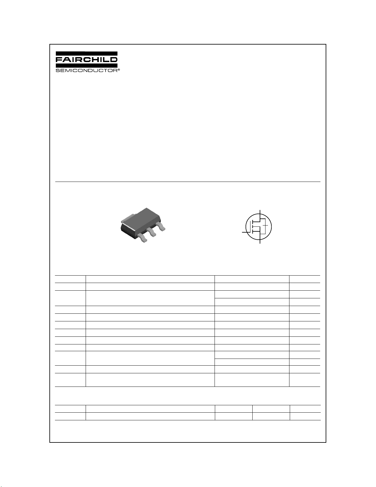
FQT7N10L
100V LOGIC N-Channel MOSFET
FQT7N10L
May 2001
TM
QFET
General Description
These N-Channel enhancement mode power field effect
transistors are produced using Fairchild’s proprietary,
planar stripe, DMOS technology.
This advanced technology has been especially tailored to
minimize on-state resistance, provide superior switching
performance, and withstand high energy pulse in the
avalanche and commutation mode. These devices are well
suited for low voltage applications such as high efficiency
Features
• 1.7A, 100V, R
• Low gate charge ( typical 4.6 nC)
• Low Crss ( typical 12 pF)
• Fast switching
• Improved dv/dt capability
• Low level gate drive requirments allowing
direct operationfrom logic drives
= 0.35Ω @VGS = 10 V
DS(on)
switching DC/DC converters, and DC motor control.
D
!
!
!
!
"
"
"
"
"
"
"
"
!
!
S
D
G
Absolute Maximum Ratings T
S
SOT-223
FQT Series
= 25°C unless otherwise noted
C
!
!
G
Symbol Parameter FQT7N10L Units
V
DSS
I
D
I
DM
V
GSS
E
AS
I
AR
E
AR
dv/dt Peak Diode Recovery dv/dt
P
D
Drain-Source Voltage 100 V
Drain Current
- Continuous (T
- Continuous (T
Drain Current - Pulsed
= 25°C)
C
= 70°C)
C
(Note 1)
1.7 A
1.36 A
6.8 A
Gate-Source Voltage ± 20 V
Single Pulsed Avalanche Energy
Avalanche Current
Repetitive Avalanche Energy
Power Dissipation (TC = 25°C)
(Note 2)
(Note 1)
(Note 1)
(Note 3)
50 mJ
1.7 A
0.2 mJ
6.0 V/ns
2.0 W
- Derate above 25°C 0.016 W/°C
T
, T
J
STG
T
L
Operating and Storage Temperature Range -55 to +150 °C
Maximum lead temperature for soldering purposes,
1/8" from case for 5 seconds
300 °C
Thermal Characteristics
Symbol Parameter Typ Max Units
R
θJA
* When mounted on the minimum pad size recommended (PCB Mount)
Thermal Resistance, Junction-to-Ambient * -- 62.5 °C/W
Rev. A, May 2001©2001 Fairchild Semiconductor Corporation
FQT7N10L
Electrical Characteristics T
= 25°C unless otherwise noted
C
Symbol Parameter Test Conditions Min Typ Max Units
Off Characteristics
BV
DSS
∆BV
DSS
/ ∆T
I
DSS
I
GSSF
I
GSSR
Drain-Source Breakdown Voltage
Breakdown Voltage Temperature
Coefficient
J
Zero Gate Voltage Drain Current
Gate-Body Leakage Current, Forward
Gate-Body Leakage Current, Reverse
= 0 V, ID = 250 µA
V
GS
I
= 250 µA, Referenced to 25°C
D
V
= 100 V, VGS = 0 V
DS
V
= 80 V, TC = 125°C
DS
V
= 20 V, VDS = 0 V
GS
= -20 V, VDS = 0 V
V
GS
100 -- -- V
-- 0.1 -- V/°C
-- -- 1 µA
-- -- 10 µA
-- -- 100 nA
-- -- -100 nA
On Characteristics
V
R
g
FS
GS(th)
DS(on)
Gate Threshold Voltage
Static Drain-Source
On-Resistance
Forward Transconductance
V
= VGS, ID = 250 µA
DS
V
= 10 V, ID = 0.85 A
GS
= 5 V, ID = 0.85 A
V
GS
V
= 30 V, ID = 0.85 A
DS
(Note 4)
1.0 -- 2.0 V
0.275
--
0.300
0.35
0.38
-- 2.75 -- S
Dynamic Characteristics
C
iss
C
oss
C
rss
Input Capacitance
Output Capacitance -- 55 72 pF
Reverse Transfer Capacitance -- 12 15 pF
= 25 V, VGS = 0 V,
V
DS
f = 1.0 MHz
-- 220 290 pF
Switching Characteristics
t
d(on)
t
r
t
d(off)
t
f
Q
Q
Q
g
gs
gd
Turn-On Delay Time
Turn-On Rise Time -- 100 210 ns
Turn-Off Delay Time -- 17 45 ns
Turn-Off Fall Time -- 50 110 ns
Total Gate Charge
Gate-Source Charge -- 1.0 -- nC
Gate-Drain Charge -- 2.6 -- nC
= 50 V, ID = 7.3 A,
V
DD
= 25 Ω
R
G
= 80 V, ID = 7.3 A,
V
DS
V
GS
= 5 V
(Note 4, 5)
(Note 4, 5)
-- 9 30 ns
-- 4.6 6.0 nC
Ω
Drain-Source Diode Characteristics and Maximum Ratings
I
S
I
SM
V
SD
t
rr
Q
rr
Notes:
1. Repetitive Rating : Pulse width limited by maximum junction temperature
2. L = 26mH, IAS = 1.7A, VDD = 25V, RG = 25 Ω, Starting TJ = 25°C
3. ISD ≤ 7.3A, di/dt ≤ 300A/µs, VDD ≤ BV
4. Pulse Test : Pulse width ≤ 300µs, Duty cycle ≤ 2%
5. Essentially independent of operating temperature
©2001 Fairchild Semiconductor Corporation
Maximum Continuous Drain-Source Diode Forward Current -- -- 1.7 A
Maximum Pulsed Drain-Source Diode Forward Current -- -- 6.8 A
= 0 V, IS = 1.7 A
Drain-Source Diode Forward Voltage
Reverse Recovery Time
Reverse Recovery Charge -- 140 -- nC
Starting TJ = 25°C
DSS,
V
GS
= 0 V, IS = 7.3 A,
V
GS
/ dt = 100 A/µs
dI
F
-- -- 1.5 V
-- 70 -- ns
(Note 4)
Rev. A, May 2001
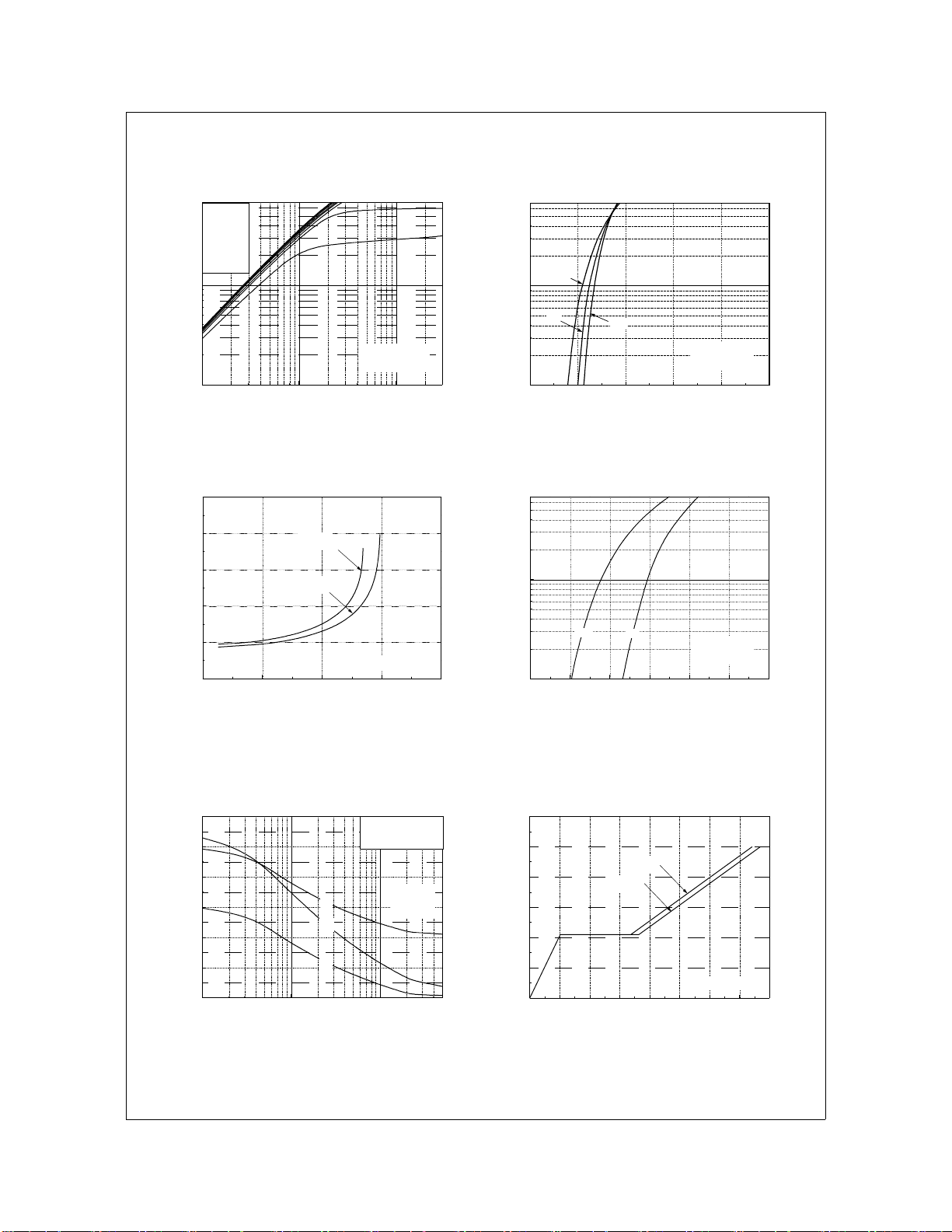
Typical Characteristics
FQT7N10L
V
GS
Top : 1 0 .0 V
8.0 V
6.0 V
5.0 V
4.5 V
4.0 V
3.5 V
Botto m : 3.0 V
0
10
, Dra in Curre n t [A ]
D
I
-1
10
-1
10
0
10
"
1. 250#s Pulse Te st
2. TC = 25
VDS, Drain-Source Voltage [V]
1.5
1.2
0.9
],
$
[
0.6
DS(ON)
R
0.3
VGS = 5V
VGS = 10V
Drain-Source On-Resistance
0.0
0 5 10 15 20
ID, Drain Current [A]
Note s :
"
10
Note : T
!
1
10
!
25
, Dra in Curre n t [A ]
D
I
-1
10
0246810
!
-55
"
Note s :
1. V
= 30V
DS
2. 250#s Pulse Tes t
!
150
0
VGS , Ga te -S ource V o ltag e [V ]
Figure 2. Transfer CharacteristicsFigure 1. On-Region Char act er i stic s
0
!
= 25
J
10
, Reverse Drain Current [A]
DR
I
-1
10
0.2 0.4 0.6 0.8 1.0 1.2 1.4
!
150
!
25
"
Note s :
= 0V
1. V
GS
2. 250#s Pulse Test
VSD , Source-Drain Voltage [V]
Figure 3. On-Resistance Variati on vs.
Drain Current and Gate Voltage
Figure 4. Body Diode Forward Voltage
Variation vs. Source Current
and Temperature
VDS = 50V
VDS = 80V
"
Note : I
600
500
400
300
200
Capacitance [pF]
100
0
-1
10
C
= Cgs + Cgd (Cds = shorted)
iss
= Cds + C
C
oss
gd
C
= C
rss
gd
"
10
1
Notes :
= 0 V
1. V
GS
2. f = 1 MH z
C
iss
C
oss
C
rss
0
10
VDS, Drain-Source Voltage [V]
12
10
8
6
4
, Gate-Source Voltage [V]
2
GS
V
0
012345678
QG, Tota l Gate Charge [n C]
Figure 5. Capacitance C haracteristics Figure 6. Gate Charge Characteristics
= 7.3 A
D
Rev. A, May 2001©2001 Fairchild Semiconductor Corporation
 Loading...