

Fairchild Semiconductor FOD2711 Datasheet
DESCRIPTION
The FOD2711 Optically Isolated Amplifier consists of the popular RC431A precision
programmable shunt reference and an optocoupler. The optocoupler is a gallium arsenide
(GaAs) light emitting diode optically coupled to a silicon phototransistor. The reference
voltage tolerance is 1%. The current transfer ratio (CTR) ranges from 100% to 200%.
It is primarily intended for use as the error amplifier/reference voltage/optocoupler
function in isolated ac to dc power supplies and dc/dc converters.
When using the FOD2711, power supply designers can reduce the component count and
save space in tightly packaged designs. The tight tolerance reference eliminates the need
for adjustments in many applications.
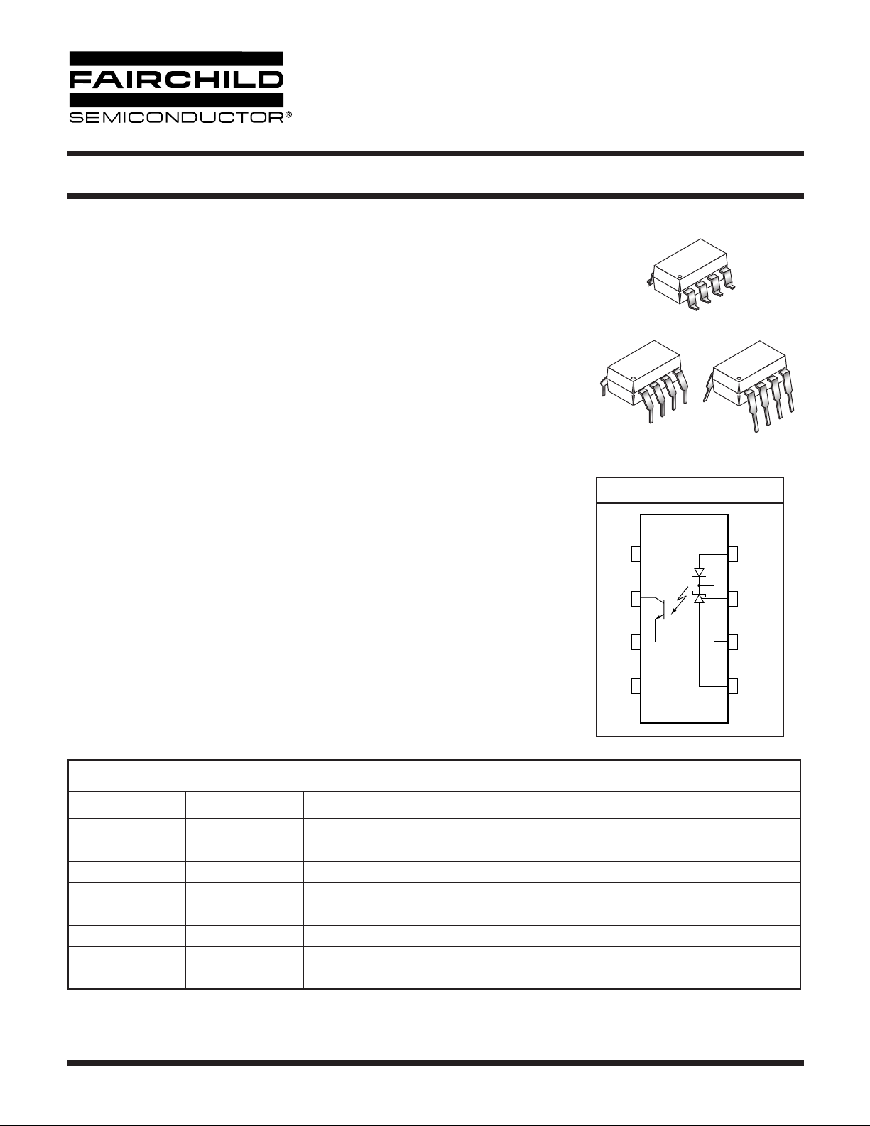
The device comes in a 8-pin dip white package.
OPTICALLY ISOLATED
ERROR AMPLIFIER
FOD2711
8
1
8
1
8
1
FEATURES
• Optocoupler, precision reference and error amplifier in single package
• 1.240V ± 1% reference
• CTR 100% to 200%
• 5,000V RMS isolation
• UL approval E90700, Volume 2
CSA approval 1296837
VDE approval 40002463
BSI approval 8702, 8703
APPLICATIONS
•Power supplies regulation
• DC to DC converters
PIN DEFINITIONS
Pin Number Pin Name Pin function description
1NCNot connected
2CPhototransistor Collector
3EPhototransistor Emitter
4NCNot connected
5 GND Ground
6 COMP Error Amplifier Compensation. This pin is the output of the error amplifier. *
7FBVoltage Feedback. This pin is the inverting input to the error amplifier
8 LED Anode LED. This pin is the input to the light emitting diode.
FUNCTIONAL BLOCK DIAGRAM
NC
1
C
2
E
3
NC
4 5
8
7
6
LED
FB
COMP
GND
* The compensation network must be attached between pins 6 and 7.
© 2003 Fairchild Semiconductor Corporation
Page 1 of 15
4/14/03
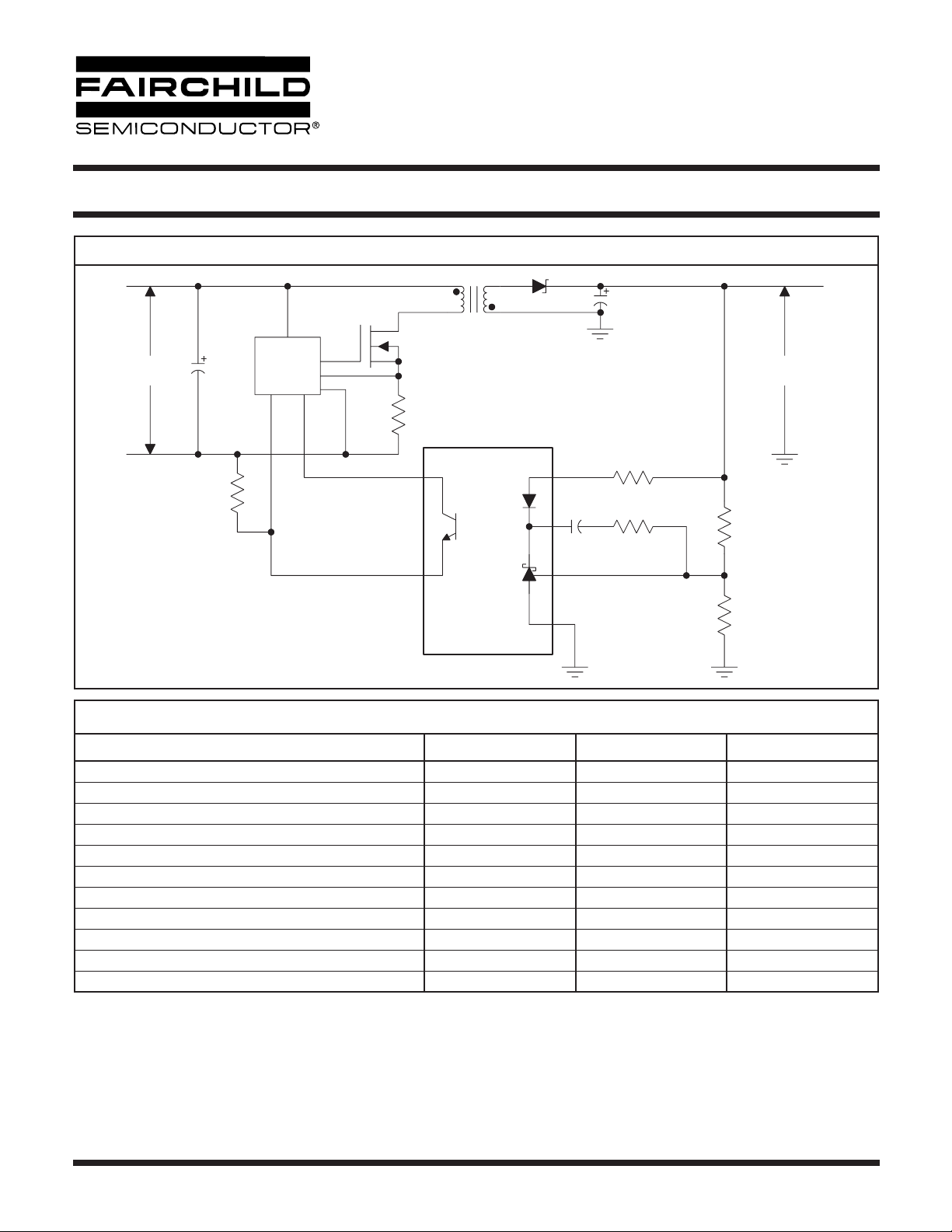
TYPICAL APPLICATION
FAN4803
V
1
PWM
Control
FOD2711
OPTICALLY ISOLATED
ERROR AMPLIFIER
FOD2711
V
O
2
3
ABSOLUTE MAXIMUM RATINGS
Parameter Symbol Value Units
Storage Temperature T
Operating Temperature T
Lead Solder Temperature T
Input Voltage V
Input DC Current I
Collector-Emitter Voltage V
Emitter-Collector Voltage V
Collector Current I
Input Power Dissipation (note 1) PD1 145 mW
Tr ansistor Power Dissipation (note 2) PD2 85 mW
Total Power Dissipation (note 3) PD3 145 mW
Notes
1. Derate linearly from 25°C at a rate of 2.42 mW/ °C
2. Derate linearly from 25°C at a rate of 1.42 mW/ °C.
3. Derate linearly from 25°C at a rate of 2.42 mW/ °C.
4. Functional operation under these conditions is not implied. Permanent damage may occur if the device is subjected to conditions
outside these ratings.
(T
= 25°C Unless otherwise specified.)
A
STG
OPR
SOL
LED
LED
CEO
ECO
8
6
7
5
-55 to +125 °C
-40 to +85 °C
260 for 10 sec. °C
13.2 V
20 mA
30 V
7V
C
50 mA
R1
R2
© 2003 Fairchild Semiconductor Corporation
Page 2 of 15
4/14/03

/ ∆
∆
/ ∆
OPTICALLY ISOLATED
ERROR AMPLIFIER
FOD2711
ELECTRICAL CHARACTERISTICS
INPUT CHARACTERISTICS
Parameter Test Conditions Symbol Min Typ** Max Unit
LED forward voltage (I
Reference voltage
(-40 to +85°C) (V
(25°C) 1.228 1.240 1.252
Deviation of V
Ratio of Vref variation
to the output of the error amplifier
Feedback input current (I
Deviation of I
Minimum drive current (V
Off-state error amplifier current (V
Error amplifier
output impedance - See Note 2
over temperature - See Note 1
REF
over temperature - See Note 1
REF
(V
(T
= 25°C Unless otherwise specified.)
A
= 10 mA, V
LED
= V
COMP
LED
, I
FB
, I
FB
= V
= 6 V, V
LED
COMP
V
= 10 mA, R1 = 10 k Ω ) (Fig.3) I
LED
= V
COMP
= V
COMP
= 10 mA (Fig.1)
LED
(T
= -40 to +85°C) V
A
(I
LED
to 12 V) (Fig.2)
REF
= -40 to +85°C) I
(T
A
= V
COMP
= 0) (Fig.4) I
FB
= 0.1 mA to 15 mA,
)(Fig.1) V
FB
= 10 mA,
) (Fig.1) I
FB
f<1 kHZ)
F
V
REF
REF (DEV)
V
REF
V
COMP
REF
REF (DEV)
LED (MIN)
(OFF)
|Z
OUT
1.221 1.259
4 12 mV
-1.5 -2.7 mV/V
0.15 0.5 µA
0.15 0.3 µA
55 80 µA
0.001 0.1 µA
| 0.25 Ohm
1.5 V
V
1. The deviation parameters V
REF(DEV)
and I
REF(DEV)
are defined as the differences between the maximum and minimum values
obtained over the rated temperature range. The average full-range temperature coefficient of the reference input voltage, ∆ V
is defined as:
A
OUT
25°C=(){}106×
| = ∆ V
COMP
I
. When the device is operating with two external resistors (see
LED
V
∆V
REF
where ∆ T
ppm/°C()
is the rated operating free-air temperature range of the device.
A
REF DEV()/VREFTA
-----------------------------------------------------------------------------------------------------=
∆T
2. The dynamic impedance is defined as |Z
Figure 2), the total dynamic impedance of the circuit is given by:
Z
OUT, TOT
∆V
=
--------Z
∆I
OUT
R1
1
--------+×≈
R2
REF
,
© 2003 Fairchild Semiconductor Corporation
Page 3 of 15
4/14/03
OPTICALLY ISOLATED
ERROR AMPLIFIER
FOD2711
OUTPUT CHARACTERISTICS
(T
= 25°C Unless otherwise specified.)
A
Parameter Test Conditions Symbol Min Typ Max Unit
Collector dark current (V
Emitter-collector voltage breakdown (I
Collector-emitter voltage breakdown (I
TRANSFER CHARACTERISTICS
(T
= 10 V) (Fig. 5) I
CE
= 100 µA) BV
E
= 1.0mA) BV
C
= 25°C Unless otherwise specified.)
A
CEO
ECO
CEO
50 nA
7V
70 V
Parameter Test Conditions Symbol Min Typ Max Unit
(I
(I
LED
LED
Current transfer ratio
Collector-emitter
saturation voltage
ISOLATION CHARACTERISTICS
= 10 mA, V
V
CE
= 10 mA, V
I
= 2.5 mA) (Fig. 6)
C
(T
= 25°C Unless otherwise specified.)
A
= V
COMP
FB
= 5 V) (Fig. 6)
= V
COMP
FB
,
CTR 100 200 %
,
V
CE
(SAT)
0.4 V
Parameter Test Conditions Symbol Min Typ Max Unit
Input-output insulation
leakage current
Withstand insulation
voltage
Resistance (input to output) V
(RH = 45%, T
V
= 3000 VDC) (note. 1)
I-O
(RH <= 50%, T
I-O
= 25°C, t = 5s,
A
= 25°C, t = 1 min)
A
(note 1)
= 500 VDC (note. 1) R
I
I-O
V
5000 Vrms
ISO
12
I-O
10
1.0 µA
Ohm
SWITCHING CHARACTERISTICS (T
= 25°C Unless otherwise specified.)
A
Parameter Test Conditions Symbol Min Typ Max Unit
Bandwidth (Fig. 7) B
Common mode transient
immunity at output high
Common mode transient
immunity at output low
= 0 mA, Vcm = 10 V
(I
LED
RL = 2.2 kΩ (Fig. 8) (note 2)
= 10 mA, Vcm = 10 V
(I
LED
RL = 2.2 kΩ (Fig. 8) (note 2)
PP
CMH 1.0 kV/µs
PP
CML 1.0 kV/µs
W
10 kHZ
Notes
1. Device is considered as a two terminal device: Pins 1, 2, 3 and 4 are shorted together and Pins 5, 6, 7 and 8 are shorted together.
2. Common mode transient immunity at output high is the maximum tolerable (positive) dVcm/dt on the leading edge of the
common mode impulse signal, Vcm, to assure that the output will remain high. Common mode transient immunity at output low
is the maximum tolerable (negative) dVcm/dt on the trailing edge of the common pulse signal,Vcm, to assure that the output will
remain low.
© 2003 Fairchild Semiconductor Corporation
Page 4 of 15
4/14/03
OPTICALLY ISOLATED
ERROR AMPLIFIER
FOD2711
I
I
(LED)
V
82
V
F
6
7
V
REF
5
3
V
R2
(LED)
8
6R1
7
V
COMP
V
REF
5
2
3
FIG. 1. V
V
, VF, I
REF
FIG. 3. I
8
6
7
5
(min) TEST CIRCUIT
LED
I
(LED)
8
I
REF
6
7
R1
5
TEST CIRCUIT
REF
2
V
3
FIG. 2. ∆V
2
3
V
REF/∆VCOMP
I
(OFF)
V
(LED)
FIG. 4. I
I
I
CEO
CE
(LED)
V
TEST CIRCUIT
(OFF)
8
6
7
V
REF
5
8
6
7
5
TEST CIRCUIT
V
COMP
2
3
I
C
2
V
CE
3
FIG. 5. I
TEST CIRCUIT FIG. 6. CTR, V
CEO
© 2003 Fairchild Semiconductor Corporation
Page 5 of 15
TEST CIRCUIT
CE(sat)
4/14/03
 Loading...