Fairchild Semiconductor FMS6410 Datasheet

www.fairchildsemi.com
FMS6410
Dual Channel Video Drivers with Integrated Filters
and Composite Video Summer
Video Features
• Dual integrated video low pass reconstruction filters on
outputs
• Composite Video Summer
• Integrated output drivers provide low impedance outputs
and deliver 2V
• 7.1MHz 4
• 7.1MHz Y and C filters, with CV out
• 42dB stopband attenuation at 27MHz on Y, C, and CV
• Better than 1dB flatness to 4.5 MHz on Y, C, and CV
• No external frequency select components or clocks
• 9ns group delay flatness on Y, C, and CV output
• AC coupled inputs and outputs
• 0.4% differential gain with 0.4 ° differential phase
• Integrated DC Restore / Clamp circuitry with low tilt
(6dB gain) video into 150 Ω .
P-P
th
order video filters
Applications
• CCTV
• Cable and Satellite Set top boxes
• DVD players
• Televisions
• Personal Video Recorders (PVRs)
• Video On Demand (VOD)
• Distribution Amplifiers
General Description
The FMS6410 Dual Channel Video Filter – Driver Chip with
CV Summer offers comprehensive video filtering for set top
box or DVD applications. This part consists of two 4
Butterworth 7.1MHz low pass filters for video signals. The
filters are optimized for low overshoot and flat group delay.
The device also contains a summing circuit to generate
filtered composite video. Integrated video drivers are
included to facilitate a direct drive to the outside world.
In a typical application, the Y and C input signals from
DACs are AC coupled into the filter. Both channels have DC
restore circuitry to clamp the DC input levels during video
sync. The Y and C channels use a separate feedback clamp.
The clamp pulse is derived from the Y channel.
The outputs are AC coupled. The Y, C and, CV outputs are
buffered to drive 2V
doubly terminated 75 Ω coax load) with up to 35pF of load
capacitance at the output pin. The Y, C, and CV channels
have a gain of approximately 2 (6dB) with 1V
levels. There is an option for the video output to be DC
coupled which limits the drive output to one output on each
channel.
into a 150 Ω load (1V
P-P
P-P
P-P
th
into a
input
order
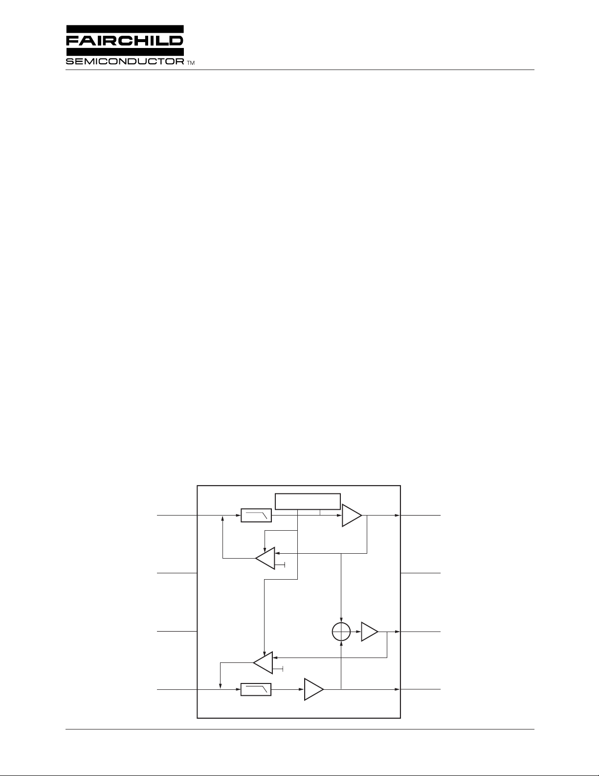
Functional Block Diagram
1
YIN
2
NC (Reserved)
3
GND_VIDEO
4
CIN
SYNC STRIP, REF,
AND TIMING
gM
1V
FMS6410
gM
1V
6dB
6dB
VCC_VIDEO
YOUT
CVOUT
COUT
8
7
6
5
REV. 0.0.2 9/3/02

FMS6410 PRODUCT SPECIFICATION
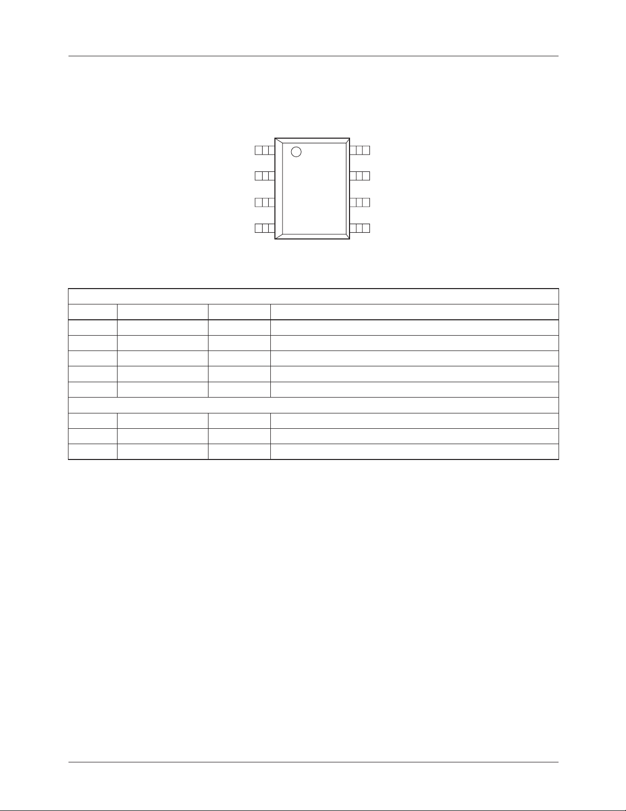
Pin Configuration
FMS6410
8-Pin SOIC (SO8
)
Video Section
Pin# Pin Type Description
1Y
4C
5C
6CV
8Y
Power/Ground Pins
7V
3 GND_VIDEO Power Ground for Video
2 NC NC Reserved (Need to Float)
YIN
NC
GND_VIDEO
CIN
IN
IN
OUT
OUT
OUT
_VIDEO Power +5 VDC for Video
CC
Input Luma (Luminance) / Composite Input
Input Chroma (Chrominance) Input
Output Filtered Chroma (Chrominance) Output
Output Summed Composite Video Output
Output Filtered Luma (Luminance) Output
1
2
3
4
8
7
6
5
YOUT
VCC_VIDEO
CVOUT
COUT
2
REV. 0.0.2 9/3/02

FMS6410
Functional Description
Introduction
The FMS6410 is a dual monolithic continuous time video
filter designed for reconstructing the luminance and chrominance signals from an S-Video D/A source. The Composite
video output is generated by summing the filtered Y and C
outputs. The chip is intended for use in applications with AC
coupled inputs and AC coupled outputs (See Figure 1). The
reconstruction filters approximate a 4th-order Butterworth
characteristic with an optimization toward low overshoot and
flat group delay. Y, C, and CV outputs are capable of driving
2V
into AC coupled 150 Ω video loads with up to 35pF of
P-P
load capacitance at the output pin. All channels are clamped
during sync to establish the appropriate output voltage swing
range. Thus the input coupling capacitors do not behave
according to the conventional RC time constant. Clamping
for all channels settles to less than 10mv within 5ms of a
change in video input sources. In most applications the input
coupling capacitors are 0.1µF. The Y and C inputs typically
sink 1µA during active video, which nominally tilts a
horizontal line by about 2mV at the Y output. During sync,
the clamp typically sources 20µA to restore the DC level.
The net result is that the average input current is zero.
Any change in the input coupling capacitor’s value will
inversely alter the amount of tilt per line. Such a change will
also linearly affect the clamp response times. This product is
robust and stable under all stated load and input conditions.
Capacitive bypassing of V
performance.
Luminance (Y) I/O
The luma input is driven by either a low impedance source of
1V
or the output of a 75 Ω terminated line. The input is
P-P
required to be AC coupled via a 0.1µF coupling capacitor
which allows for a settling time of 5ms. The luma output is
capable of driving an AC coupled 150 Ω load at 2V
1V
into a doubly terminated 75 Ω load. Up to 35pF of
P-P
load capacitance (at the output pin) can be driven without
stability or slew issues. The output is AC coupled with a
220µF or larger AC coupling capacitor.
directly to ground ensures this
CC
P-P
, or
Chrominance (C) I/O
The chroma input is driven by a low impedance source of
0.7V
required to be AC coupled via a 0.1µF coupling capacitor
which allows for a clamp setting time of 5ms. The chroma
output is capable of driving an AC coupled 150 Ω load at
2V
35pF of load capacitance can be driven without stability or
slew issues. A 0.1µF AC coupling capacitor is recommended
at the output. Since chrominance signals do not contain
low frequency components, the smaller 0.1µF cap is
recommended instead of the 220µF cap to reduce circuit
cost.
or the output of a 75 Ω terminated line. The input is
P-P
P-P
, or 1V
into a doubly terminated 75 Ω load. Up to
P-P
Composite Video (CV) Output
The composite video output is capable of driving 2 loads to
2V
. It is intended to drive a TV and a VCR. Either the TV
P-P
input or the VCR input can be shorted to ground and the
other output will still meet specifications. Up to 35pF of load
capacitance (at the output pin) can be driven without stability
or slew issues.
DC Coupled Output Applications
The 220µF capacitor coupled with the 150 Ω termination
forms a high pass filter that blocks the DC while passing the
video frequencies and avoiding tilt. Lower values such as
10µF would create a problem. By AC coupling, the average
DC level is zero. Thus, the output voltages of all channels
will be centered around zero. Alternately, DC coupling the
output of the FMS6410 is allowable. There are several
tradeoffs: The average DC level on the outputs will be 2V;
Each output will dissipate an additional 40mW nominally;
The application will need to accommodate a 1V DC offset
sync tip; And it is recommended to limit each output to one
150 Ω load.
REV. 0.0.2 9/3/02
3
 Loading...