

Fairchild Semiconductor FMBA06 Datasheet
Discrete POWER & Signal
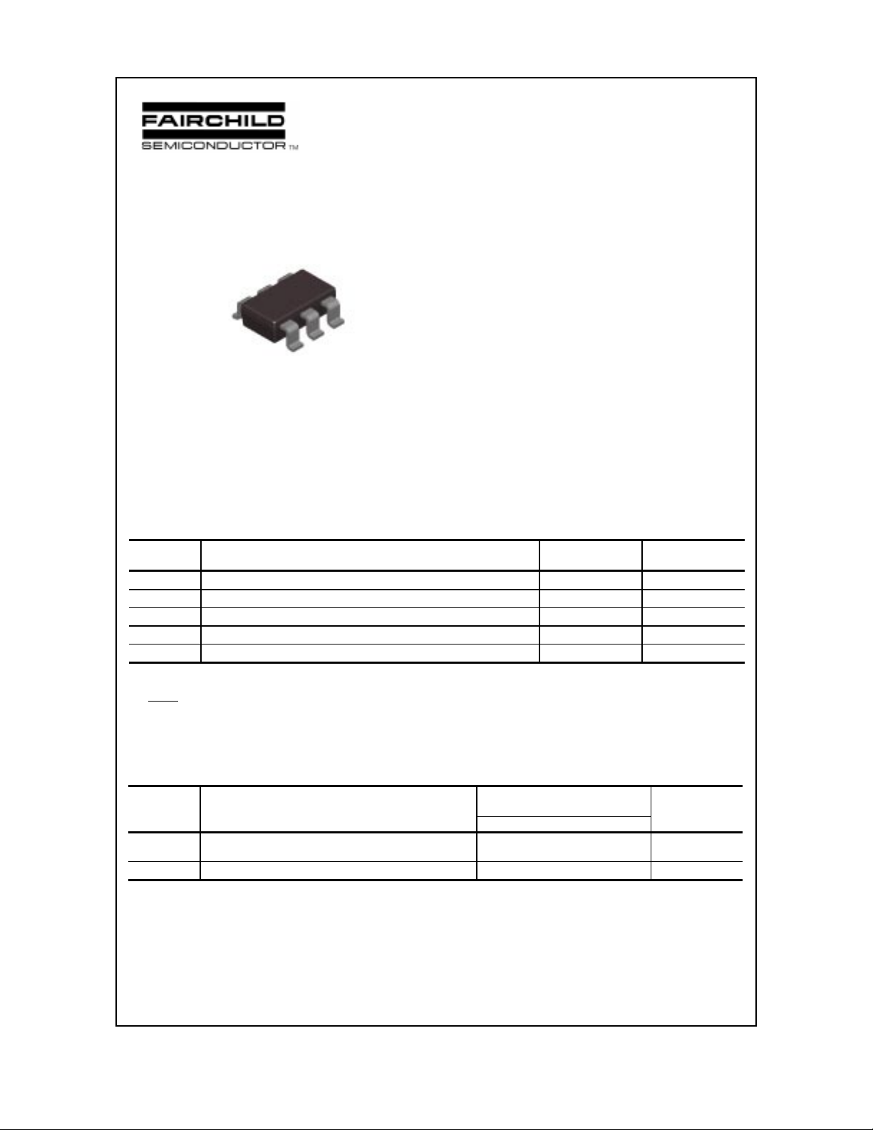
FMBA06
C2
E1
C1
B2
E2
B1
pin #1
SuperSOT-6
Mark: .1G
NPN Multi-Chip General Purpose Amplifier
This device is designed for general purpose amplifier applications at collector
currents to 300 mA. Sourced from Process 33.
FMBA06
Technologies
Absolute Maximum Ratings* T
= 25°C unless otherwise noted
A
Symbol Parameter Value Units
V
CEO
V
CBO
V
EBO
I
C
TJ, T
stg
Collector-Emitter Voltage 80 V
Collector-Base Voltage 80 V
Emitter-Base Voltage 4.0 V
Collector Current - Continuous 500 mA
Operating and Storage Junction Temperature Range -55 to +150
°
C
*These ratings are limiting values above which the serviceability of any semiconductor device may be impaired.
NOTES:
1) These ratings are based on a maximum junction temperature of 150 degrees C.
2) These are steady state limits. The factory should be consulted on applications involving pulsed or low duty cycle operations.
Thermal Characteristics T
= 25°C unless otherwise noted
A
Symbol Characteristic Max Units
FMBA06
P
D
R
θ
JA
Total Device Dissipation
Derate above 25°C
700
5.6
Thermal Resistance, Junction to Ambient 180
mW
mW/°C
°C/W
1998 Fairchild Semiconductor Corporation
NPN Multi-Chip General Purpose Amplifier
(continued)
FMBA06
Electrical Characteristics T
= 25°C unless otherwise noted
A
Symbol Parameter Test Conditions Min Typ Max Units
OFF CHARACTERISTICS
V
(BR)CEO
V
(BR)EBO
I
CEO
I
CBO
Collector-Emitter Sustaining Voltage* IC = 1.0 mA, IB = 0 80 V
Emitter-Base B reakdown Voltage
I
= 100 µA, IC = 0
E
4.0 V
Collector-Cutoff Current VCE = 60 V, IB = 0 0.1
Collector-Cutoff Current VCB = 80 V, IE = 0 0.1
µA
µA
ON CHARACTERISTICS
h
FE
V
V
sat
CE(
BE(on)
DC Current Gain IC = 10 mA, VCE = 1.0 V
= 100 mA, VCE = 1.0 V
I
Collector-Em i tter Saturation Voltage IC = 100 mA, IB = 10 mA 0.25 V
)
C
Base-Emitter On Voltage IC = 100 mA, VCE = 1.0 V 1.2 V
100
100
SMALL SIGNAL CHARACTERISTICS
f
T
Current Gain - Bandwidth Product IC = 10 mA, VCE = 2.0 V,
f = 100 MHz
150 MHz
*Pulse Test: Pulse Width ≤ 300 µs, Duty Cycle ≤ 2.0%
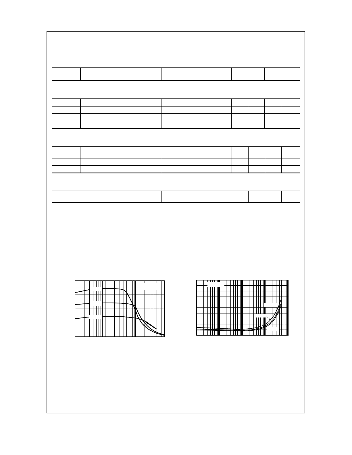
Typical Characteristics
T ypical Pulsed Current Gain
vs Collector Current
200
125 °C
150
25 °C
100
- 40 ºC
50
0.001 0.01 0.1
FE
h - TYPICAL PULSED CURRENT GAIN
I - COLLECTOR CURRENT (A)
C
V = 1V
CE
Collector-Emitter Saturation
Voltage vs Collector Current
- COLLECTOR EMITTER VOLTAGE (V)
CESAT
0.5
0.4
0.3
0.2
0.1
β
= 10
125 °C
25 °C
- 40 ºC
0
0.1 1 10 100 1000
I - COLLECTOR CURRENT (mA)
C
 Loading...