

Fairchild Semiconductor FMB3906 Datasheet
FFB3906 / FMB3906 / MMPQ3906
g
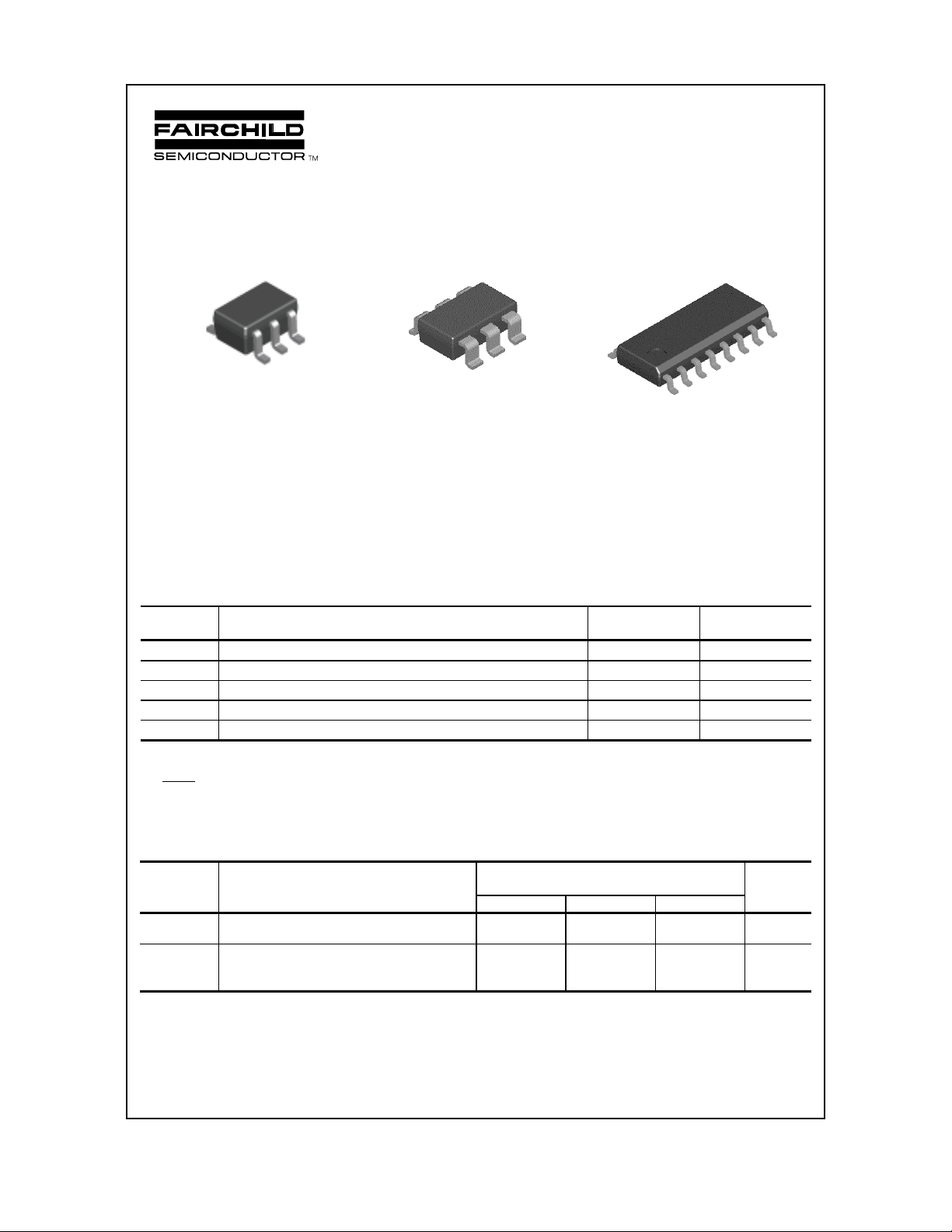
FFB3906
E2
B2
C1
SC70-6
Mark: .2A
NOTE: The pinouts are symmetrical; pin 1 and pin
4 are interchangeable. Units inside the carrier can
be of either orientation and will not affect the
functionality of the device.
pin #1
C2
B1
E1
FMB3906
C2
E1
C1
B1
pin #1
SuperSOT-6
Mark: .2A
B2
E2
Mark: MMPQ3906
MMPQ3906
B3
E3
B2
E2
B1
E1
C1
SOIC-16
pin #1
B4
E4
C3
C3
C2
C2
C1
PNP Multi-Chip General Purpose Amplifier
This device is designed for general purpose amplifier and switching
applications at collector currents of 10 µA to 100 mA. Sourced
from Process 66.
Absolute Maximum Ratings* T
Symbol Parameter Value Units
V
CEO
V
CBO
V
EBO
I
C
TJ, T
st
*These ratings are limiting values above which the serviceability of any semiconductor device may be impaired.
NOTES:
1) These ratings are based on a maximum junction temperature of 150 degrees C.
2) These are steady state limits. The factory should be consulted on applications involving pulsed or low duty cycle operations.
Collector-Emitt er Vol t age 40 V
Collector-Base Voltage 40 V
Emitter-Base Voltage 5.0 V
Collector Current - Continuous 200 mA
Operating and Stora ge Junction Temperature Range -55 to +150
= 25°C unless otherwise noted
A
C
°
C4
C4
Thermal Characteristics T
= 25°C unless otherwise noted
A
Symbol Characteristic Max Units
FFB3904 FMB3904 MMPQ3904
P
D
R
θ
JA
1998 Fairchild Semiconductor Corporation
Total Device Dissipation
Derate above 25°C
Thermal Resistance, Junction to Ambient
Effective 4 Die
Each Die
300
2.4
700
5.6
415 180
1,000
8.0
125
240
mW
mW/°C
°
C/W
°
C/W
°
C/W
PNP Multi-Chip General Purpose Amplifier
(continued)
FFB3906 / FMB3906 / MMPQ3906
Electrical Characteristics T
= 25°C unless otherwise noted
A
Symbol Parameter Test Conditions Min Typ Max Units
OFF CHARACTERISTICS
V
(BR)CEO
V
(BR)CBO
V
(BR)EBO
I
BL
I
CEX
Collector-Emitter Breakdown
IC = 1.0 mA, IB = 0 40 V
Voltage*
Collector-Base Breakdown Vol tage
Emitter-Base B reakdown Voltage
I
= 10 µA, IE = 0
C
I
= 10 µA, IC = 0
E
Base Cutoff Current VCE = 30 V, V
= 3.0 V 50 nA
BE
40 V
5.0 V
Collector Cutoff Current VCE = 30 V, VBE = 3.0 V 50 nA
ON CHARACTERISTICS
h
FE
V
V
CE(sat)
BE(sat)
DC Current Gain * IC = 0.1 mA, VCE = 1.0 V
= 1.0 mA, VCE = 1.0 V
I
C
= 10 mA, VCE = 1.0 V
I
C
= 50 mA, VCE = 1.0 V
I
C
= 100 mA, VCE = 1.0 V
I
C
Collector-Emitter Saturation Voltage IC = 10 mA, IB = 1.0 mA
= 50 mA, IB = 5.0 mA
I
C
Base-Emitter Saturation Voltage IC = 10 mA, IB = 1.0 mA
= 50 mA, IB = 5.0 mA
I
C
60
80
100
300
60
30
0.25
0.4
0.65 0.85
0.95
SMALL SIGNAL CHARACTERISTICS
f
T
C
obo
C
ibo
NF Noise Figure
Current Gain - Bandwidth Product IC = 10 mA, VCE = 20 V,
f = 100 MHz
Output Capacitance VCB = 5.0 V, IE = 0,
f = 100 kHz
Input Capacitance VEB = 0.5 V, IC = 0,
f = 100 kHz
(except MMPQ3906)
IC = 100 µA, VCE = 5.0 V,
=1.0kΩ, f=10 Hz to 15.7 kHz
R
S
450 MHz
3.0 pF
8.0 pF
2.5 dB
V
V
V
V
SWITCHING CHARACTERISTICS
t
d
t
r
t
s
t
f
*
Pulse T est: Pulse Width ≤ 300 µs, Duty Cycle ≤ 2.0%
Delay Time VCC = 3.0 V, VBE = 0.5 V, 15 ns
Rise Time IC = 10 mA, IB1 = 1.0 mA 20 ns
Storage Time VCC = 3.0 V, IC = 10mA 110 ns
Fall Time IB1 = IB2 = 1.0 mA 40 ns
Spice Model
PNP (Is=1.41f Xti=3 Eg=1.11 Vaf=18.7 Bf=180.7 Ne=1.5 Ise=0 Ikf=80m Xtb=1.5 Br=4.977 Nc=2 Isc=0 Ikr=0
Rc=2.5 Cjc=9.728p Mjc=.5776 Vjc=.75 Fc=.5 Cje=8.063p Mje=.3677 Vje=.75 Tr=33.42n Tf=179.3p Itf=.4 Vtf=4
Xtf=6 Rb=10)
 Loading...