

Fairchild Semiconductor FM803T Datasheet
1
www.fairchildsemi.com
FM803 3-Pin
µ
C Supervisor Device
www.fairchildsemi.com
FM803 Rev. C.3
FM803
3-Pin
µC Supervisor Device
General Description
The FM803 is a supervisory device designed to monitor power
supply or other system voltage. FM803 generates a reset pulse
whenever the voltage being monitored is out of tolerance. Once
asserted, the reset pulse is guaranteed to be valid for a minimum
of 140ms (256ms typical ). The reset output of FM803 is of active
low Open-Drain type and has an internal pull-up resistor.
Several threshold voltages are offered to accommodate 5.0V,
3.3V, 3.0V and 2.7V system voltages.
These devices are offered in space saving 3-pin SOT23 and SC70
packages.
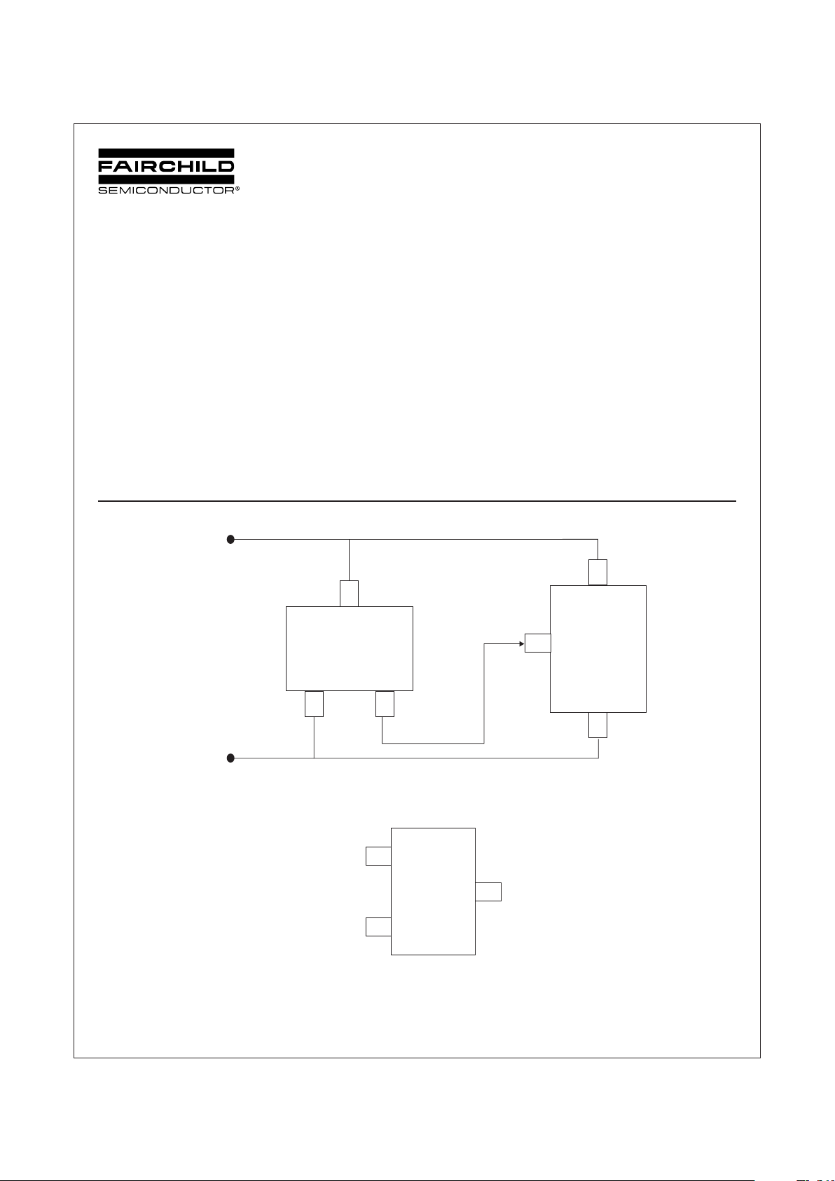
Typical Operating Circuit
October 2002
Features
■ Automatic reset generation on power-up
■ Minimum 140 ms reset pulse
■ Internal 5kΩ pull-up resistor
■ Other reset pulse choices available: 32 - 256 ms
■ Operating temperature
-40°C to + 105°C (SOT-23)
-40°C to +85°C (SC70)
■ Choice of Reset Thresholds: 4.63V, 4.38V, 4.00V, 3.08V,
2.93V, 2.63V
■ SOT23-3 and SC70-3 Packages
© 2000 Fairchild Semiconductor International
Connection Diagram
GND
V
CC
/RESET
1
FM803
2
3
SC70-3 & SOT23-3 Packages
1
FM803
Controller
2
3
V
CC
GND
/RESET
2
www.fairchildsemi.com
FM803 3-Pin
µ
C Supervisor Device
www.fairchildsemi.com
FM803 Rev. C.3
Absolute Maximum Ratings
Voltage on any terminal relative to GND
V
CC
-0.3V to +6.0V
/RESET -0.3V to +6.0V
Input Current 20mA
Output Current: /RESET 20mA
Rate of Rise of V
CC
100V/µs
Continuous Power Dissipation (T
A
= +70°C)
SOT23-3 (derate 4mW/°C above +70°C) 320mW
Operating Temperature Range -40°C to +105°C
Storage Temperature Range -65°C to +150°C
Lead Temperature (soldering, 10s) +300°C
These are stress ratings only, and functional operation is not implied for these levels or beyond. Exposure to Absolute Maximum Rating
conditions for extended periods may affect device reliability.
Electrical Characteristics SOT-23 Package (T
A
= 25°C unless otherwise noted)
VCC = full range, as noted under conditions. See Note 1.
Parameter Symbol Conditions Min Typ Max Units
(Note 2)
Operating Voltage V
CC
TA = -40°C to +105°C 1.1 5.5 V
Supply Current I
CC
TA = -40°C to +105°C, VCC < 5.5V 5 10 µA
FM803J/L/M
T
A
= -40°C to +105°C, VCC < 3.6V 3 6
FM803R/S/T
Reset Threshold V
TH
FM803L TA = -40°C to +105°C 4.40 4.63 4.86 V
FM803M TA = -40°C to +105°C 4.18 4.38 4.52
FM803J TA = -40°C to +105°C 3.90 4.00 4.18
FM803T TA = -40°C to +105°C 2.97 3.08 3.19
FM803S TA = -40°C to +105°C 2.79 2.93 3.00
FM803R TA = -40°C to +105°C 2.49 2.63 2.70
Reset Threshold Tempco 30 ppm/°C
VCC to Reset Delay VCC = VTH to (VTH - 100mV) 10 µs
Reset Active Timout Period TA = -40°C to +105°C 140 256 560 ms
FM803 Output Low V
OL
VCC = VTH(min), I
SINK
= 1.2mA, 0.3 V
FM803R/S/T
VCC = VTH(min), I
SINK
= 3.2mA, 0.4
FM803J/L/M
VCC = < 1.0V, I
SINK
= 50µA 0.3
Open-Drain Output Leakage VCC > VTH(max), I
RESET
= 1 0.8V
CC
1 µA
Current
Note 1: Testing in production is 25°C only. Limits over temperature are guaranteed by design.
Note 2: Typical values are at 25°C.
Note 3: Recommended minimum slew rate for the VCC rampup is 200mV/sec in the 0 to 2V range for the device to function properly.
3
www.fairchildsemi.com
FM803 3-Pin
µ
C Supervisor Device
www.fairchildsemi.com
FM803 Rev. C.3
Absolute Maximum Ratings
Voltage on any terminal relative to GND
V
CC
-0.3V to +6.0V
/RESET -0.3V to (V
CC
+ 0.3V)
Input Current 20mA
Output Current: /RESET 20mA
Rate of Rise of V
CC
100V/µs
Continuous Power Dissipation (T
A
= +70°C)
SC70-3 174mW
Operating Temperature Range -40°C to +85°C
Storage Temperature Range -65°C to +150°C
Lead Temperature (soldering, 10s) +300°C
These are stress ratings only, and functional operation is not implied for these levels or beyond. Exposure to Absolute Maximum Rating
conditions for extended periods may affect device reliability.
Electrical Characteristics SC70 Package (T
A
= 25°C unless otherwise noted)
VCC = full range, as noted under conditions. See Note 1.
Parameter Symbol Conditions Min Typ Max Units
(Note 2)
Operating Voltage V
CC
TA = 0°C to +70°C 1.4 5.5 V
TA = -40°C to +85°C 1.6 5.5
Supply Current I
CC
TA = -40°C to +85°C, VCC < 5.5V 9 15 µA
FM803J/L/M
TA = -40°C to +85°C, VCC < 3.6V 6 10
FM803R/S/T
Reset Threshold V
TH
FM803L TA = -40°C to +85°C 4.40 4.63 4.86 V
FM803M TA = -40°C to +85°C 4.18 4.38 4.52
FM803J TA = -40°C to +85°C 3.90 4.00 4.18
FM803T TA = -40°C to +85°C 2.97 3.08 3.19
FM803S TA = -40°C to +85°C 2.79 2.93 3.00
FM803R TA = -40°C to +85°C 2.49 2.63 2.70
Reset Threshold Tempco 30 ppm/°C
VCC to Reset Delay (Note 2) VCC = VTH to (VTH - 100mV) 10 µs
Reset Active Timout Period TA = -40°C to +85°C 140 256 560 ms
FM803 Output Low V
OL
VCC = VTH(min), I
SINK
= 1.2mA, 0.35 V
FM803R/S/T
VCC = VTH(min), I
SINK
= 3.2mA, 0.4
FM803J/L/M
VCC = < 1.0V, I
SINK
= 50µA 0.3
Open-Drain Output Leakage VCC > VTH(max), /RESET = 1 7 µA
Current
Note 1: Testing in production is 25°C only. VCC = 5V for FM803L/M/J, VCC = 3.3V for FM803T/S and VCC = 3V for FM803R. Limits over temperature are guaranteed by design.
Note 2 Typical values are at 25°C.
 Loading...