

Fairchild Semiconductor FM3560 Datasheet
1
www.fairchildsemi.com
FM3540/60
4/5 Bit Multiplexed, 1 Bit Latched Port with Standard 2-Wire Bus Interface and Non-Volatile Latches
www.fairchildsemi.com
FM3540/60 Rev. C
FM3540/60
4/5 Bit Multiplexed, 1 Bit Latched Port with Standard
2-Wire Bus Interface and Non-Volatile Latches
General Description
The FM3540/60 multiplexes the I-port input signals with two
internal non-volatile registers that can be loaded through the serial
port. The multiplexer is selected via the serial port and defaults to
the I-Port upon power-up. Pull-up resistors are provided on the
input port to accommodate connections to open drain outputs and
to eliminate the need for external resistors. The device supports
a choice of either 2.5V output or Open Drain Outputs for easy
interface to devices with different VDD Levels.
The serial port is an IIC compatible slave only interface and
supports both 100kbits and 400kbits modes of operation. The port
is used to read the I-Port, Write Data to the internal non-volatile
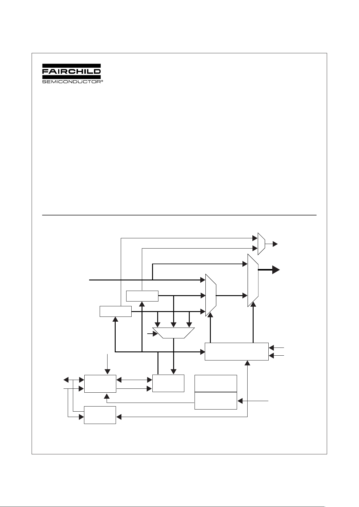
Block Diagram
October 2001
registers and select whether the I-Port or one of the internal nonvolatile registers is output to the Y-port. The FM3540/60 is
fabricated with an advanced CMOS technology to achieve high
density and low power.
Features
■ Extended Operating Voltage Range 3.0V-5.5V
■ IIC Compatible Slave Interface.
■ ESD performance: Human body model > 2000V
■ Choice of 2.5V outputs or Open-Drain Outputs
© 2001 Fairchild Semiconductor Corporation
SOPRA
SOPRB
IIC
Interface
Start/Stop
Logic
Shift
Register
Slave Address
Register
Comparator
Control Logic
Mux3
Mux2
Non_Mux_Out
Y[4:0]
I[4:0]
IIC Read Logic
SDA
SCL
ASEL
OVRD
MUXSEL
MXSB, MXSA
Mux1

2
www.fairchildsemi.com
FM3540/60
4/5 Bit Multiplexed, 1 Bit Latched Port with Standard 2-Wire Bus Interface and Non-Volatile Latches
www.fairchildsemi.com
FM3540/60 Rev. C
SDA 1 14 SCL
I0 2 13 VCC
I1 3 12 Y0
I2 4 11 Y1
I3 5 10 Y2
I4 6 9Y3
GND 7 8Y4
SCL 1 20 V
CC
SDA 2 19 ASEL
OVRD 3 18 WP
I0 4 17 Non_Mux_Out
I1 5 16 MUXSEL
I2 6 15 Y0
I3 7 14 Y1
I4 8 13 Y2
Level 9 12 Y3
GND 10 11 Y4
Ordering Information
Order Package Package Y-Port Device
Number Number Description Packing Output Type Address
FM3540CM14 M14A 14-Pin SO T&R Open-Collector 1001110
FM3540CMT14 MTC14 14-Pin TSSOP T&R Open-Collector 1001110
FM3540SM14 M14A 14-Pin SO T&R Fixed 2.5V 1001110
FM3540SMT14 MTC14 14-Pin TSSOP T&R Fixed 2.5V 1001110
FM3560M20 M20B 20-Pin SO T&R (See Note below) (See Note below)
FM3560MT20 MTC20 20-Pin TSSOP T&R (See Note below) (See Note below)
Note About Y-Port Output Type:
FM3560 device has a dedicated input pin (LEVEL) to select either "Fixed 2.5Volts" or "Open-Collector" Y-Port output type.
Note About Device Address:
1. For FM3540 with an alternate device address of 0110111, contact Fairchild Marketing/Sales.
2. FM3560 device has a dedicated input pin (ASEL) to select either "1001110" or 0110111" as device address.
Pin Connection Diagrams
14-Pin Packages
FM3540
20-Pin Packages
FM3560
Pin Description
Pin Name Description
I[0:4] Data Inputs w/Pullups (10K-40K)
Y[0:4] O/D Data Outputs
SCL Serial Port Clock Input (120K pullup)
Override# Override Input, sets all outputs to 0
WP Write Protect Input
Non_Mux_Out Non-Multiplexed Output
Mux_Sel Mux. Select Input
Level Level Select Input
ASEL Address Select Input
SDA Serial Port Data I/O (120K pullup)

3
www.fairchildsemi.com
FM3540/60
4/5 Bit Multiplexed, 1 Bit Latched Port with Standard 2-Wire Bus Interface and Non-Volatile Latches
www.fairchildsemi.com
FM3540/60 Rev. C
Functional Description
The FM3540/60 has two primary functional modes of operation
and an additional mode for programming the device.
Operational Modes
During standard operation the device will either pass an address
to the Y-Port from the I-Port or from an internally programmed
value. At power up the device will default to passing the I-Port
value to the Y-Port.
The I-port values are generated from the motherboard of the
system and may be hardwired or driven by another device. Pullup resistors are provided on the device to accommodate this
device being driven by open drain output drivers. The device
expects standard CMOS input signals. The level of the output
signal is determined by the Level input. If this input is connected
to Vss/Ground, the output is at 2.5V on the multiplexed outputs
(Y0-Y4). The non-multiplexed output is always at CMOS levels.
The Level input, if left unconnected (it has an internal pullup), will
cause the Y0-Y4 outputs to operate as open-drain outputs. The
override# input, when set to 0, will cause all the outputs to be set
to 0. The WP signal, if set to logic 1, will prevent data from being
written to the non-volatile register.
The mux_sel input, when set to logic 0, will select the data from the
non-volatile register to drive on the Y0-4 outputs. If set to logic 1,
the data from the inputs are selected instead. The non_mux_out
latch is transparent when the mux_sel signal is at logic 0, and will
latch data when the mux_select is in a logic 1 state.
Output Port: Y0-Y4
The output port is an open drain output to allow for easy connection to devices running at different voltage levels. The port is
always active and either passes the value on the I-Port or the value
in the Serial output port Register (SOPR). Changing the Mux Path
is accomplished by writing to b7, b6 of the Serial Input Port
Register. SOPR-b7, b6 defaults to a value of "10" at power up and
the default path is from the I-Port through to the output port. The
multiplexer only updates when an IIC stop condition is observed.
Register Description
The FM3540/60 has 3 registers in total. These registers are made
up of a combination of read only, write only and read write bits. The
two registers are listed below.
Serial Output Port Register A(SOPRA) Address: 00H
- A read/
write register that contains the new value to be written to output
Port-Y and the multiplexer select bit.
Serial Output Port Register B(SOPRB) Address: 01H
- A read/
write register that contains the new value to be written to output
Port-Y and the multiplexer select bit.
Parallel Input Port Register (PIPR) Address: 02H
- A read only
register that is loaded with the 5 bit value of the I-Port.
Serial Output Port Register (SOPR)
(Address 000b and 001b)
MXSB MXSA Data Field
0 0 I5 NMO I3 I2 I1 I0
b7 b6 b5 b4 b3 b2 B1 b0
b7-b6 - Multiplexer Select Bits (MXSB,MXSA)
00 - Multiplexer passes the SOPR(A).
01 - Multiplexer passer the SOPR(B).
10 - Multiplexer defaults to passing the I-Port Value.
b5, b3-b0 - Data Field. New value to be output through the
multiplexer.
nmo - Non multiplexed output from internal non-volatile bit
Parallel Input Port Register (PIPR)
(Address 002b)
Address Field Data Field
0 0 0 I4 I3I2I1 I0
b7 b6 b5 b4 b3 b2 B1 b0
b7-b5 - Address field. Value is always 000
b4-b0 - Data Field. Value is equal to the value on the I-Port.
The external Port Register captures the value on the I-Port. Data
is latched into this register on the first clock after a start condition
is seen. This insures that a valid value will always be in this register
if it is read. This register is a read only register with respect to the
IIC port.
Over- mux_ Non_
ride# sel MXSB MXSA mux_outputs mux_output
0 0 X X all 0's all 0's
0 1 X X Mux_inputs latched NMO
(see note 1)
1 0 1 0 Mux_inputs latched NMO
(see note 1)
1 0 0 0 From Non- From non-
volatile reg- volatile reg-
ister (SOPRA) ister (SOPRA)
1 0 1 1 Do not use this combination
1 0 0 1 From Non- From non-
volatile reg- volatile reg-
ister (SOPRB) ister (SOPRB)
1 1 Note 2 Note 1 Mux_inputs From Non-
volatile reg-
ister (SOPRA
or SOPRB)
Note 1: Latched NMO state will be the value present on the NMO output at the time
of the mux_sel input transitioning from logic 0 to logic 1 state.
Note 2: Output depends on previously selected state of MXSB and MXSA bits
written to device.
 Loading...