

Fairchild Semiconductor FM34W02UL, FM34W02U Datasheet
May 2001
FM34W02U
2K-Bit Standard 2-Wire Bus Interface Serial EEPROM
with Full Array Write Protect
Designed with Permanent Write-Protection for First 128 Bytes for Serial Presence
Detect Application on Memory Modules (PC100/PC133 Compliant)
with Full Array Write Protect
FM34W02U 2K-Bit Standard 2-Wire Bus Interface Serial EEPROM
General Description
The FM34W02U is 2048 bits of CMOS non-volatile electrically
erasable memory. This device is specifically designed to support
Serial Presence Detect circuitry in memory modules. This communications protocol uses CLOCK (SCL) and DATA I/O (SDA)
lines to synchronously clock data between the master (for example a microprocessor) and the slave EEPROM device(s).
The contents of the non-volatile memory allows the CPU to
determine the capacity of the module and the electrical characteristics of the memory devices it contains. This will enable "plug and
play" capability as the module is read and PC main memory
resources utilized through the memory controller.
The first 128 bytes of the memory of the FM34W02U can be
permanently Write Protected by writing to the "WRITE PROTECT"
Register. Write Protect implementation details are described
under the section titled Addressing the WP Register.
The FM34W02U is available in a JEDEC standard TSSOP package for low profile memory modules for systems requiring efficient
space utilization such as in a notebook computer. Two options are
available: L - Low Voltage and LZ - Low Power, allowing the part
to be used in systems where battery life is of primary importance.
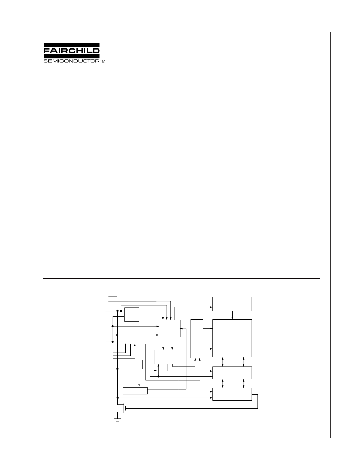
Block Diagram
V
CC
V
SS
WP
SDA
SCL
A2
A1
A0
START
STOP
LOGIC
SLAVE ADDRESS
REGISTER &
COMPARATOR
Write Protect
Register
CONTROL
LOGIC
LOAD INC
WORD
ADDRESS
COUNTER
R/W
Device Address Bits
D
IN
Features
■ PC100/PC133 Compliant
■ Extended Operating Voltage: 2.7V-5.5V
■ Software Write-Protection for first 128 bytes
■ Hardware Write-Protection for entire memory array
■ 200 µA active current typical
– 1.0 µA standby current typical (L)
– 0.1 µA standby current typical (LZ)
■ IIC compatible interface
– Provides bidirectional data transfer protocol
■ Sixteen byte page write mode
– Minimizes total write time per byte
■ Self timed write cycle
- Typical write cycle time of 6ms
■ Endurance: 1,000,000 data changes
■ Data retention greater than 40 years
■ Packages available: 8-pin TSSOP and 8-pin SO
■ Temperature Ranges: Commercial and Extended
0/1/2/3
4
TIMING &CONTROL
16
H.V. GENERATION
E2PROM
ARRAY
16 x 16 x 8
16
YDEC
8
DATA REGISTER
D
OUT
START CYCLE
XDEC
4
CK
© 2001 Fairchild Semiconductor Corporation
FM34W02U Rev. A.1
1
www.fairchildsemi.com
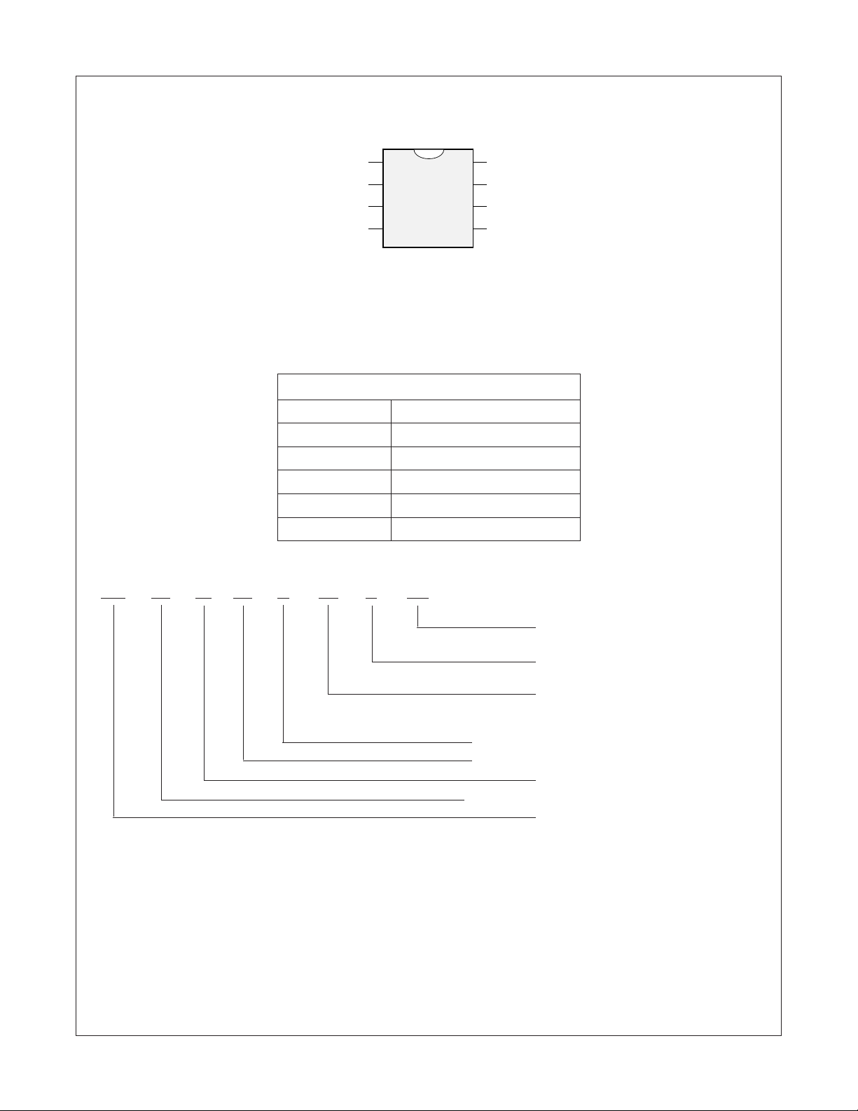
Connection Diagram
SO (M8) and TSSOP (MT8) Package
A0
A1
1
2
V
8
CC
WP
7
FM34W02U
A2
3
V
SS
4
SCL
6
SDA
5
Top View
See Package Number
M08A and MTC08
Pin Names
A0,A1,A2 Device Address Inputs
V
SS
SDA Data I/O
SCL Clock Input
WP Write Protect
V
CC
Ground
Power Supply
with Full Array Write Protect
FM34W02U 2K-Bit Standard 2-Wire Bus Interface Serial EEPROM
Ordering Information
FM 34 W 02 U LZ E XX Letter Description
Package M8 8-Pin SO8
Temp. Range None 0 to 70°C
Voltage Operating Range Blank 4.5V to 5.5V
Process U Ultralite CS100UL
Density 02 2K
Interface 34 IIC
MT8 8-Pin TSSOP
E -40 to +85°C
L 2.7V to 5.5V
LZ 2.7V to 5.5V and
<1µA Standby Current
W Full Array Write Protect
FM Fairchild Non-Volatile
Memory
FM34W02U Rev. A.1
2
www.fairchildsemi.com
Product Specifications
with Full Array Write Protect
FM34W02U 2K-Bit Standard 2-Wire Bus Interface Serial EEPROM
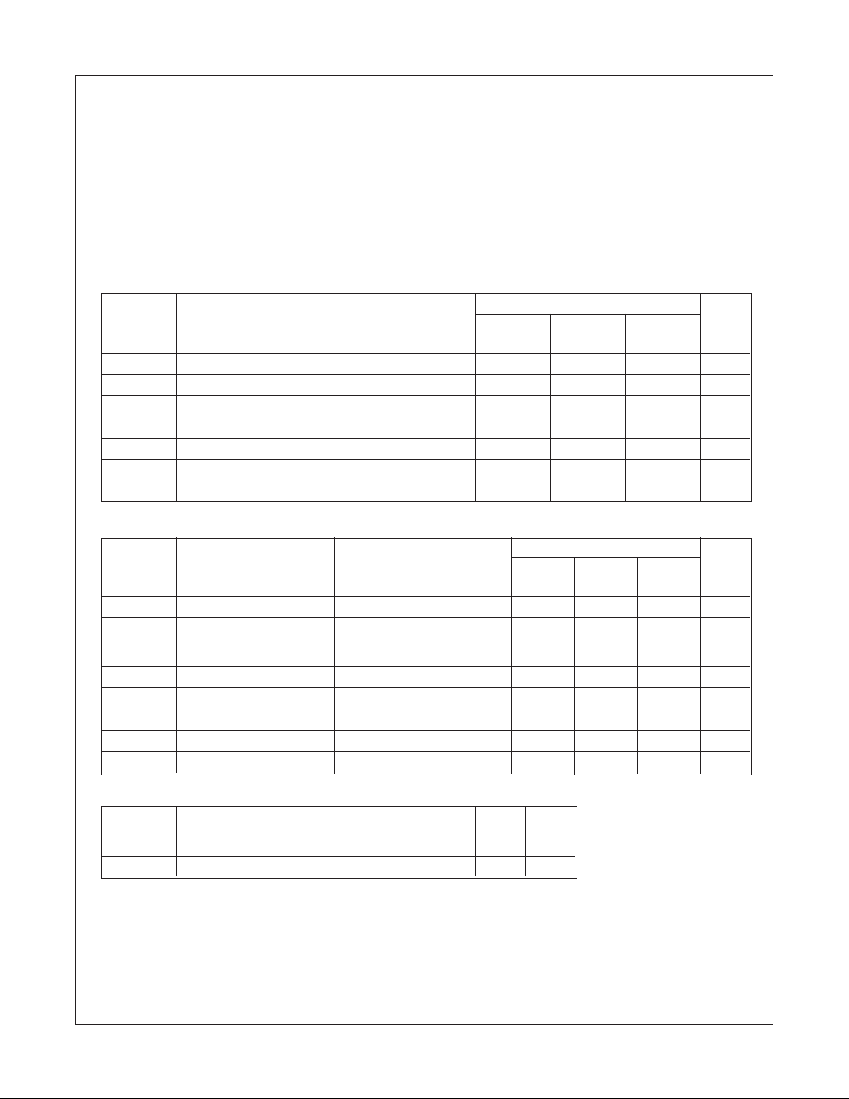
Absolute Maximum Ratings
Ambient Storage Temperature –65°C to +150°C
All Input or Output Voltages
with Respect to Ground 6.5V to –0.3V
Lead Temperature
(Soldering, 10 seconds) +300°C
ESD Rating 2000V min.
Operating Conditions
Ambient Operating Temperature
FM34W02U 0°C to +70°C
FM34W02UE -40°C to +85°C
Positive Power Supply
FM34W02U 4.5V to 5.5V
FM34W02UL 2.7V to 5.5V
FM34W02ULZ 2.7V to 5.5V
Standard VCC (4.5V to 5.5V) DC Electrical Characteristics
Symbol Parameter Test Conditions Limits Units
Min Typ Max
(Note 1)
I
V
V
CCA
I
SB
I
LI
I
LO
V
OL
IL
IH
Active Power Supply Current f
Standby Current VIN = GND or V
Input Leakage Current VIN = GND to V
Output Leakage Current V
= 400 kHz 0.2 1.0 mA
SCL
10 50 µA
0.1 1 µA
0.1 1 µA
= GND to V
OUT
CC
CC
CC
Input Low Voltage –0.3 VCC x 0.3 V
Input High Voltage VCC x 0.7 VCC + 0.5 V
Output Low Voltage I
= 3 mA 0.4 V
OL
Low VCC (2.7V to 5.5V) DC Electrical Characteristics
Symbol Parameter Test Conditions Limits Units
Min Typ Max
(Note 1)
I
CCA
I
SB
I
LI
I
LO
V
IL
V
IH
V
OL
Capacitance T
Active Power Supply Current f
= 400 kHz 0.2 1.0 mA
SCL
Standby Current VIN = GND or VCC = 4.5V - 5.5V 10 50 µA
VIN = GND or VCC = 2.7V - 5.5V (L) 1 10 µA
VIN = GND or VCC = 2.7V - 5.5V (LV) 0.1 1 µA
Input Leakage Current VIN = GND to V
Output Leakage Current V
= GND to V
OUT
CC
CC
Input Low Voltage –0.3 V
0.1 1 µA
0.1 1 µA
x 0.3 V
CC
Input High Voltage VCC x 0.7 VCC + 0.5 V
Output Low Voltage IOL = 3 mA 0.4 V
= +25°C, f = 100/400 KHz, VCC = 5V (Note 2)
A
Symbol Test Conditions Max Units
C
I/O
C
IN
Note 1: Typical values are TA = 25°C and nominal supply voltage (5V).
Note 2: This parameter is periodically sampled and not 100% tested.
Input/Output Capacitance (SDA) V
= 0V 8 pF
I/O
Input Capacitance (A0, A1, A2, SCL) VIN = 0V 6 pF
FM34W02U Rev. A.1
3
www.fairchildsemi.com
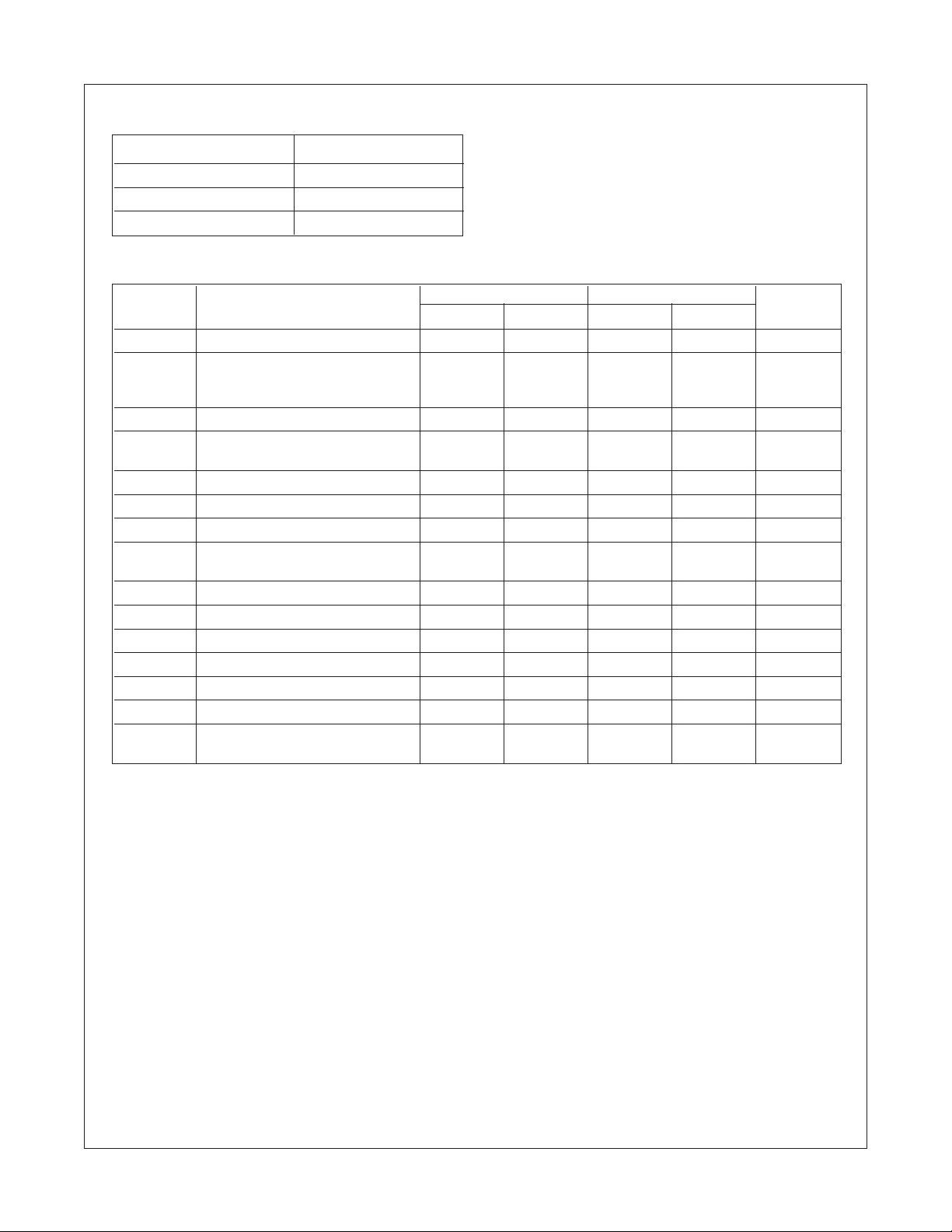
AC Conditions of Test
Input Pulse Levels VCC x 0.1 to VCC x 0.9
Input Rise and Fall Times 10 ns
Input & Output Timing Levels VCC x 0.5
Output Load 1 TTL Gate and CL = 100 pF
Read and Write Cycle Limits (Standard and Low VCC Range 2.7V - 5.5V)
Symbol Parameter 100 KHz 400 KHz Units
Min Max Min Max
f
SCL
T
I
t
AA
t
BUF
t
HD:STA
t
LOW
t
HIGH
t
SU:STA
t
HD:DAT
t
SU:DAT
t
R
t
F
t
SU:STO
t
DH
t
WR
(Note 3) - FM34W02UL, FM34W02ULZ 15 15
SCL Clock Frequency 100 400 KHz
Noise Suppression Time Constant at
SCL, SDA Inputs (Minimum V
IN
100 50 ns
Pulse width)
SCL Low to SDA Data Out Valid 0.3 3.5 0.1 0.9 µs
Time the Bus Must Be Free before 4.7 1.3 µs
a New Transmission Can Start
Start Condition Hold Time 4.0 0.6 µs
Clock Low Period 4.7 1.5 µs
Clock High Period 4.0 0.6 µs
Start Condition Setup Time 4.7 0.6 µs
(for a Repeated Start Condition)
Data in Hold Time 0 0 ns
Data in Setup Time 250 100 ns
SDA and SCL Rise Time 1 0.3 µs
SDA and SCL Fall Time 300 300 ns
Stop Condition Setup Time 4.7 0.6 µs
Data Out Hold Time 300 50 ns
Write Cycle Time - FM34W02U 10 10 ms
with Full Array Write Protect
FM34W02U 2K-Bit Standard 2-Wire Bus Interface Serial EEPROM
Note 3: The write cycle time (tWR) is the time from a valid stop condition of a write sequence to the end of the internal erase/program cycle. During the write cycle, the
FM34W02U bus interface circuits are disabled, SDA is allowed to remain high per the bus-level pull-up resistor, and the device does not respond to its slave address.
4
FM34W02U Rev. A.1
www.fairchildsemi.com
 Loading...