

Fairchild Semiconductor FM27C040NE120, FM27C040N90, FM27C040N150, FM27C040N120 Datasheet
1
www.fairchildsemi.com
NM27C040 Rev. C.1
NM27C040 4,194,304-Bit (512K x 8) High Performance CMOS EPROM
NM27C040
4,194,304-Bit (512K x 8) High Performance
CMOS EPROM
General Description
The NM27C040 is a high performance, 4,194,304-bit Electrically
Programmable UV Erasable Read Only Memory. It is organized
as 512K words of 8 bits each. Its pin-compatibility with byte-wide
JEDEC EPROMs enables upgrades through 8 Mbit EPROMs.
The “Don’t Care” feature on VPP during read operations allows
memory expansions from 1M to 8 Mbits with no printed circuit
board changes.
The NM27C040 provides microprocessor-based systems extensive storage capacity for large portions of operating system and
application software. Its 120ns access time provides high speed
operation with high-performance CPUs. The NM27C040 offers a
single chip solution for the code storage requirements of 100%
firmware-based equipment. Frequently used software routines
are quickly executed from EPROM storage, greatly enhancing
system utility.
The NM27C040 is manufactured using Fairchild’s advanced
CMOS AMG™ EPROM technology.
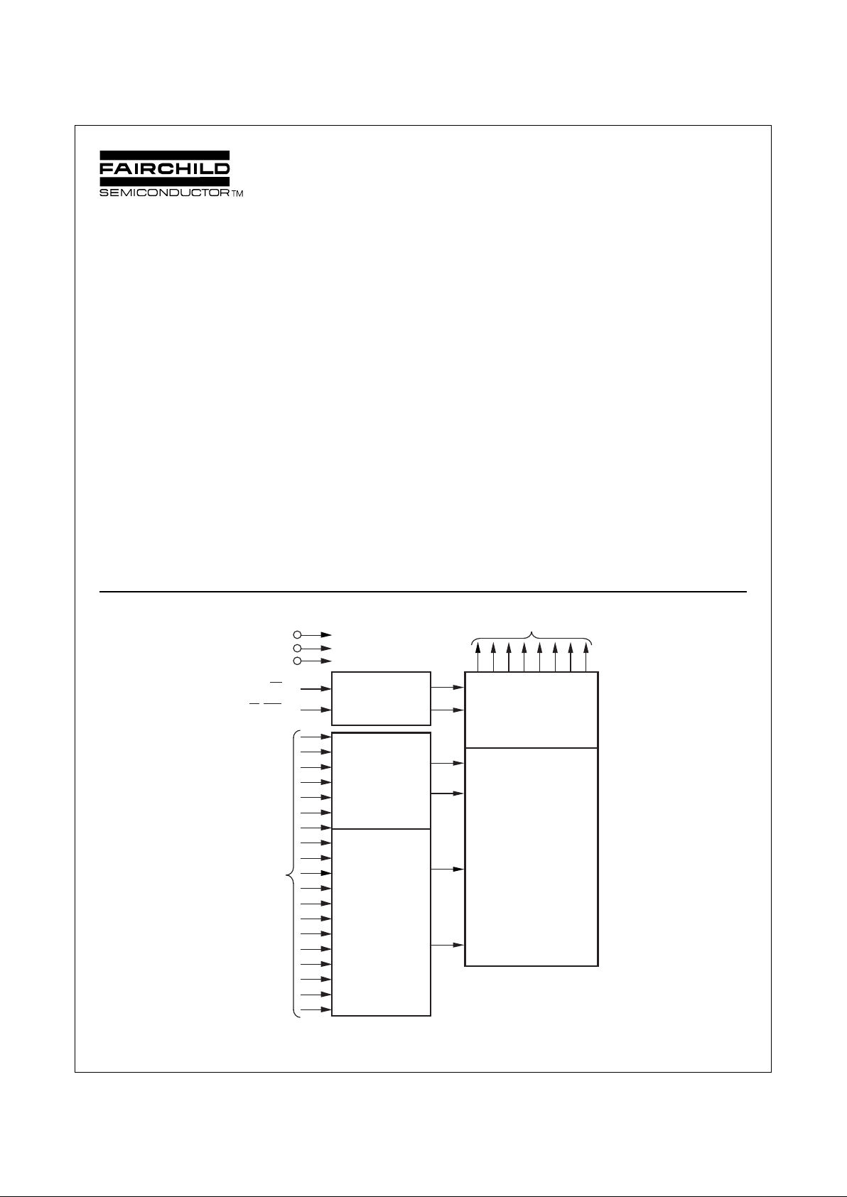
Block Diagram
February 1999
Features
■ High performance CMOS
—120, 150ns access time*
■ Simplified upgrade path
—VPP is a “Don’t Care” during normal read operation
■ Manufacturer’s identification code
■ JEDEC standard pin configuration
—32-pin PDIP
—32-pin PLCC
—32-pin CERDIP
DS010836-1
AMG™ is a trademark of WSI, Inc.
© 1999 Fairchild Semiconductor Corporation
Output Enable,
Chip Enable, and
Program Logic
Y Decoder
X Decoder
. . . . . . . . .
Output
Buffers
Y Gating
4,194,304-Bit
Cell Matrix
Data Outputs O0 - O
7
V
CC
GND
V
PP
OE
CE/PGM
A0 - A
18
Address
Inputs
*Note: New revision meets 70ns. Please check with factory for availability.
2
www.fairchildsemi.com
NM27C040 Rev. C.1
NM27C040 4,194,304-Bit (512K x 8) High Performance CMOS EPROM
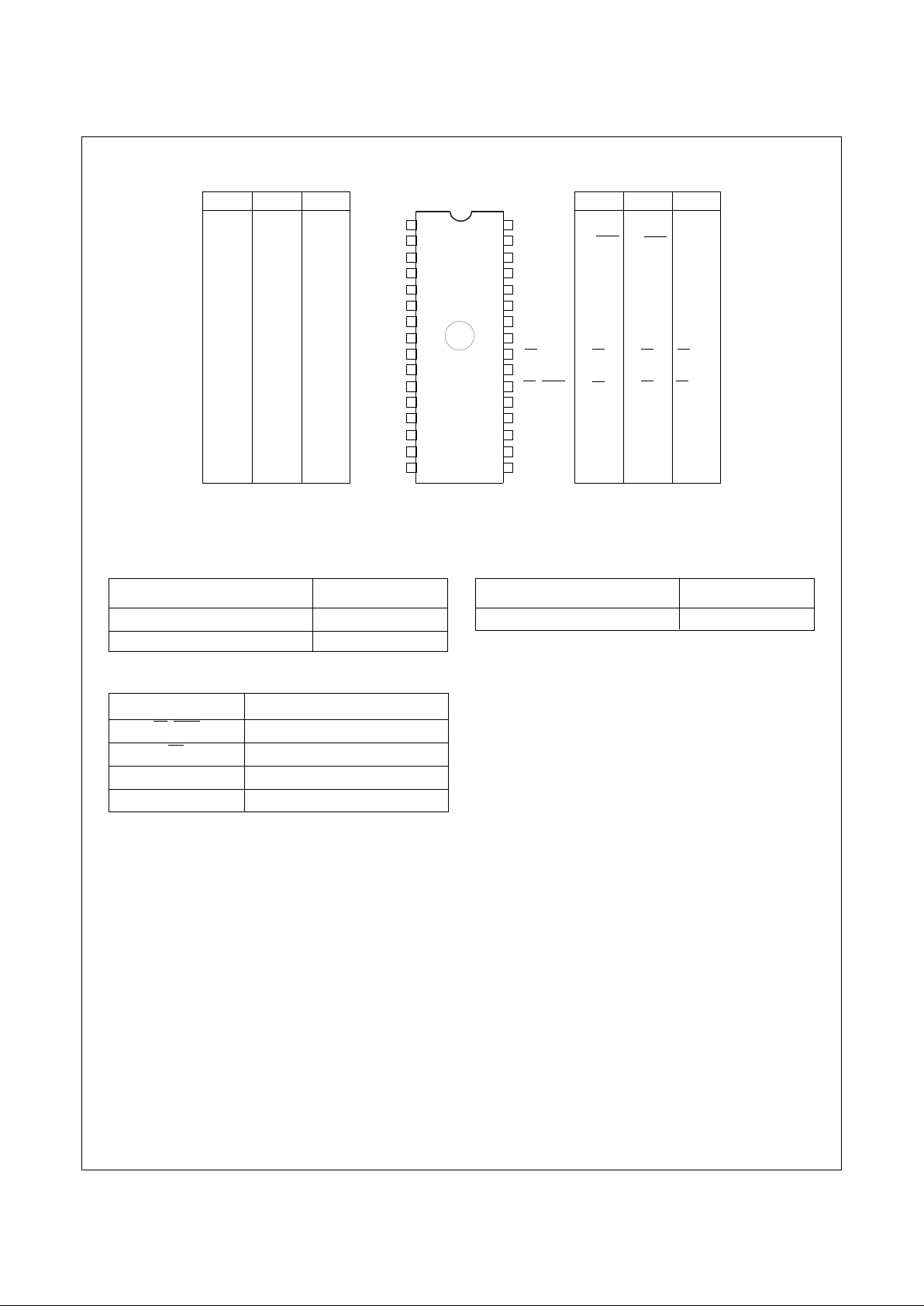
Connection Diagrams
Note: Compatible EPROM pin configurations are shown in the blocks adjacent to the NM27C040 pin.
Commercial Temperature Range
(0°C to +70°C) VCC = 5V ±10%
Parameter/Order Number Access Time (ns)
NM27C040 Q, N, V 120 120
NM27C040 Q, N, V 150 150
Extended Temperature Range
(-40°C to +85°C) VCC = 5V ±10%
Parameter/Order Number Access Time (ns)
NM27C040 QE, NE, VE 150 150
Package Types: NM27C040 Q, N,V XXX
Q = Quartz-Windowed Ceramic DIP
N = Plastic DIP
V = PLCC
• All packages conform to the JEDEC standard.
• All versions are guaranteed to function for slower speeds.
Pin Names
A0–A18 Addresses
CE/PGM Chip Enable/Program
OE Output Enable
O0–O7 Outputs
XX Don’t Care (During Read)
1
2
3
4
5
6
7
8
9
10
11
12
13
14
15
16
32
31
30
29
28
27
26
25
24
23
22
21
20
19
18
17
XX/V
PP
A
16
A
15
A
12
A
7
A
6
A
5
A
4
A
3
A
2
A
1
A
0
O
0
O
1
O
2
GND
XX/V
PP
A
16
A
15
A
12
A
7
A
6
A
5
A
4
A
3
A
2
A
1
A
0
O
0
O
1
O
2
GND
A
19
A
16
A
15
A
12
A
7
A
6
A
5
A
4
A
3
A
2
A
1
A
0
O
0
O
1
O
2
GND
27C020 27C010
XX/V
PP
A
16
A
15
A
12
A
7
A
6
A
5
A
4
A
3
A
2
A
1
A
0
O
0
O
1
O
2
GND
27C010 27C020
NM27C040
V
CC
A
18
A
17
A
14
A
13
A
8
A
9
A
11
OE
A
10
CE/PGM
O
7
O
6
O
5
O
4
O
3
V
CC
XX/PGM
NC
A
14
A
13
A
8
A
9
A
11
OE
A
10
CE
O
7
O
6
O
5
O
4
O
3
V
CC
XX/PGM
A
17
A
14
A
13
A
8
A
9
A
11
OE
A
10
CE
O
7
O
6
O
5
O
4
O
3
27C080
V
CC
A
18
A
17
A
14
A
13
A
8
A
9
A
11
OE/V
PP
A
10
CE/PGM
O
7
O
6
O
5
O
4
O
3
27C080
DS010836-2
3
www.fairchildsemi.com
NM27C040 Rev. C.1
NM27C040 4,194,304-Bit (512K x 8) High Performance CMOS EPROM
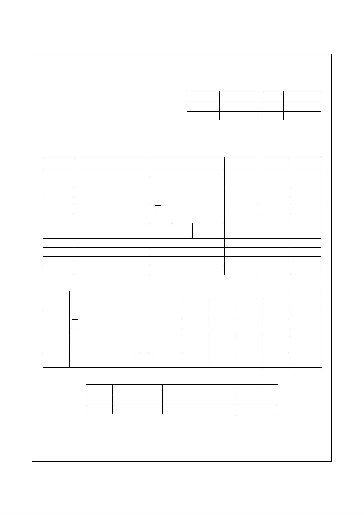
Absolute Maximum Ratings (Note 1)
Storage Temperature -65°C to +150°C
All Input Voltages except A9 with
Respect to Ground -0.6V to +7V
VPP and A9 with Respect to Ground -0.6V to +14V
VCC Supply Voltage with
Respect to Ground -0.6V to +7V
ESD Protection >2000V
All Output Voltages with
Respect to Ground VCC +1.0V to GND - 0.6V
Operating Range
Range Temperature V
CC
Tolerance
Commercial 0°C to +70°C +5V ±10%
Industrial -40°C to +85°C +5V ±10%
Read Operation
DC Electrical Characteristics Over operating range with V
PP
= V
CC
Symbol Parameter Test Conditions Min Max Units
V
IL
Input Low Level -0.5 0.8 V
V
IH
Input High Level 2.0 VCC +1 V
V
OL
Output Low Voltage IOL = 2.1 mA 0.4 V
V
OH
Output High Voltage IOH = -2.5 mA 3.5 V
I
SB1
VCC Standby Current (CMOS) CE = VCC ± 0.3V 100 µA
I
SB2
VCC Standby Current CE = V
IH
1mA
I
CC
VCC Active Current CE = OE = VIL, f=5 MHz 30 mA
I/O = 0 mA
I
PP
VPP Supply Current VPP = V
CC
10 µA
V
PP
VPP Read Voltage VCC - 0.4 V
CC
V
I
LI
Input Load Current VIN = 5.5V or GND -1 1 µA
I
LO
Output Leakage Current V
OUT
= 5.5V or GND -10 10 µA
AC Electrical Characteristics Over operating range with V
PP
= V
CC
Symbol Parameter 120 150 Units
Min Max Min Max
t
ACC
Address to Output Delay 120 150
t
CE
CE to Output Delay 120 150
t
OE
OE to Output Delay 50 50
t
DF
Output Disable to 45 55 ns
(Note 2) Output Float
t
OH
Output Hold from Addresses CE or OE , 0 0
(Note 2) Whichever Occurred First
Capacitance T
A
= +25°C, f = 1 MHz (Note 2)
Symbol Parameter Conditions Typ Max Units
C
IN
Input Capacitance VIN = 0V 9 15 pF
C
OUT
Output Capacitance V
OUT
= 0V 12 15 pF
4
www.fairchildsemi.com
NM27C040 Rev. C.1
NM27C040 4,194,304-Bit (512K x 8) High Performance CMOS EPROM
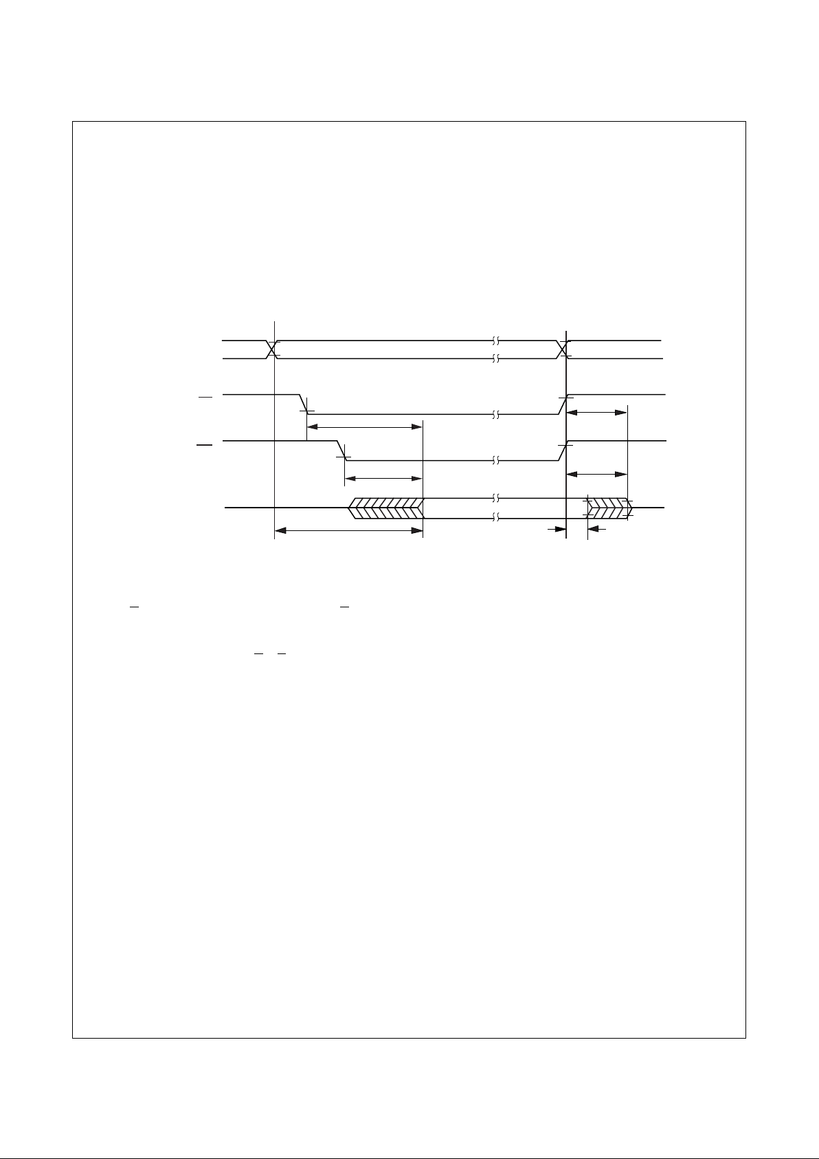
AC Test Conditions
Output Load 1 TTL Gate and CL = 100 pF (Note 8)
Input Rise and Fall Times ≤5 ns
Input Pulse Levels 0.45V to 2.4V
Timing Measurement Reference Level (Note 10)
Inputs 0.8V and 2V
Outputs` 0.8V and 2V
AC Waveforms (Notes 6, 7, 9)
Note 1: Stresses above those listed under “Absolute Maximum Ratings” may cause permanent damage to the device. This is a stress rating only and functional operation of
the device at these or any other conditions above those indicated in the operational sections of this specification is not implied. Exposure to absolute maximum rating conditions
for extended periods may affect device reliability.
Note 2: This parameter is only sampled and is not 100% tested.
Note 3: OE may be delayed up to t
ACC
- tOE after the falling edge of CE without impacting t
ACC
.
Note 4: The tDF and tCF compare level is determined as follows:
High to TRI-STATE®, the measured V
OH1
(DC) - 0.10V;
Low to TRI-STATE, the measured V
OL1
(DC) + 0.10V.
Note 5: TRI-STATE may be attained using OE or CE .
Note 6: The power switching characteristics of EPROMs require careful device decoupling. It is recommended that at least a 0.1 µF ceramic capacitor be used on every device
between VCC and GND.
Note 7: The outputs must be restricted to VCC + 1.0V to avoid latch-up and device damage.
Note 8: 1 TTL Gate: IOL = 1.6 mA, IOH = -400 µA.
CL: 100 pF includes fixture capacitance.
Note 9: VPP may be connected to VCC except during programming.
Note 10:Inputs and outputs can undershoot to -2.0V for 20 ns Max.
Addresses Valid
Valid Output
Hi-Z
2V
0.8V
2V
0.8V
2V
0.8V
ADDRESSES
OUTPUT
CE
OE
t
CE
2V
0.8V
(Note 3)
(Note 3)
t
DF
(Note 4, 5)
(Note 4, 5)
t
OH
Hi-Z
t
OE
ACC
t
CF
t
DS010836-4
 Loading...