

Fairchild Semiconductor FM27C010T45L, FM27C010T45, FM27C010QE150, FM27C010QE120, FM27C010Q90 Datasheet
...
1
www.fairchildsemi.com
FM27C010 1,048,576-Bit (128K x 8) High Performance CMOS EPROM
www.fairchildsemi.com
FM27C010
FM27C010
1,048,576-Bit (128K x 8) High Performance
CMOS EPROM
General Description
The FM27C010 is a high performance, 1,048,576-bit Electrically
Programmable UV Erasable Read Only Memory. It is organized
as 128K-words of 8 bits each. Its pin-compatibility with byte-wide
JEDEC EPROMs enables upgrades through 8 Mbit EPROMs.
The “Don’t Care” feature during read operations allows memory
expansions from 1M to 8M bits with no printed circuit board
changes.
The FM27C010 can directly replace lower density 28-pin EPROMs
by adding an A16 address line and V
CC
jumper. During the normal
read operation PGM and V
PP
are in a “Don’t Care” state which
allows higher order addresses, such as A17, A18, and A19 to be
connected without affecting the normal read operation. This
allows memory upgrades to 8M bits without hardware changes.
The FM27C010 is also offered in a 32-pin plastic DIP with the
same upgrade path.
The FM27C010 provides microprocessor-based systems extensive storage capacity for large portions of operating system and
application software. Its 70 ns access time provides no-wait-state
operation with high-performance CPUs. The FM27C010 offers a
single chip solution for the code storage requirements of 100%
firmware-based equipment. Frequently-used software routines
are quickly executed from EPROM storage, greatly enhancing
system utility.
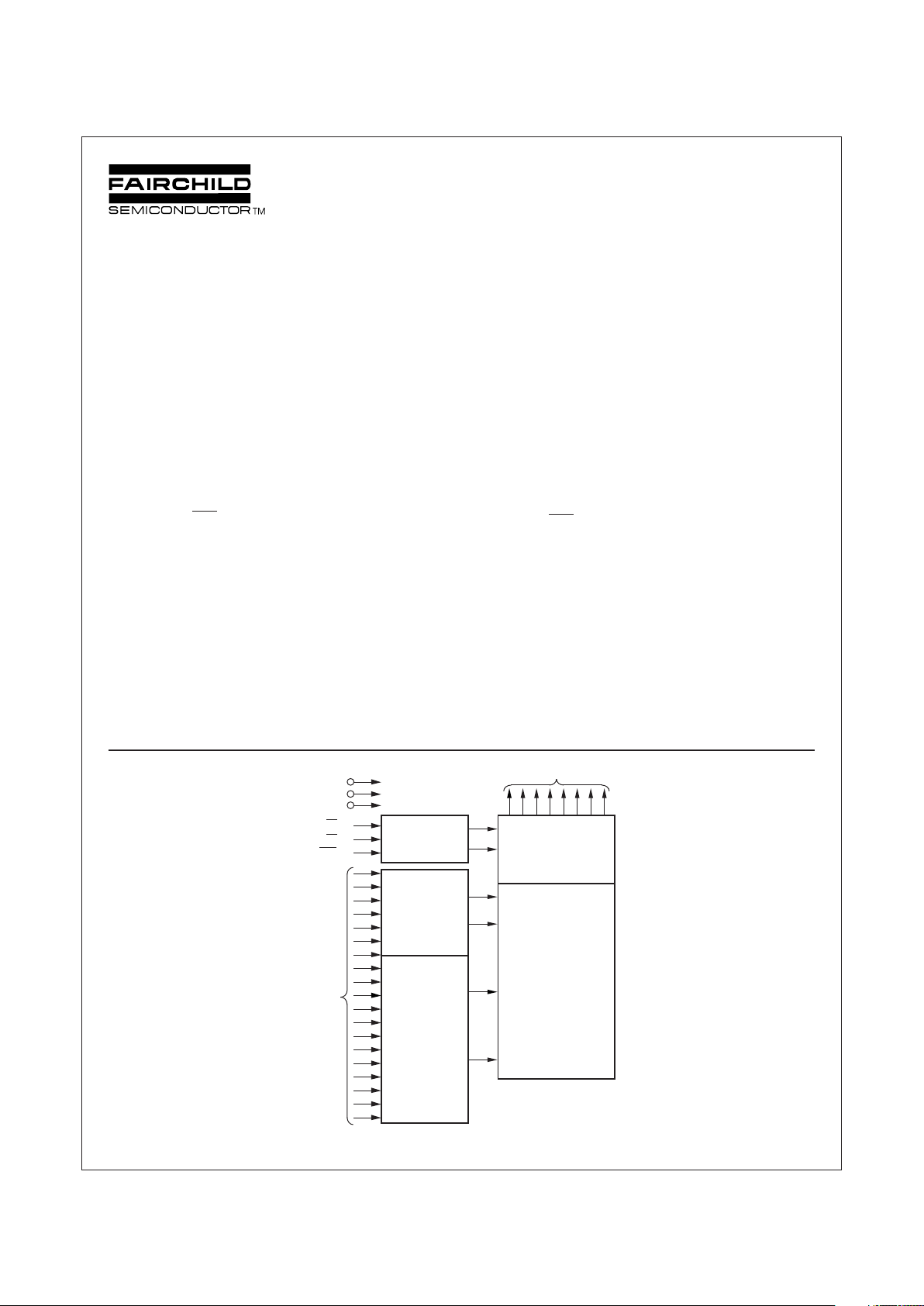
Block Diagram
January 2000
The FM27C010 is manufactured using Fairchild’s advanced CMOS
AMG™ EPROM technology.
The FM27C010 is one member of a high density EPROM Family
which range in densities up to 4 Megabit.
Features
■ High performance CMOS
—70 ns access time
■ Fast turn-off for microprocessor compatibility
■ Simplified upgrade path
—VPP and PGM are “Don’t Care” during normal read
operation
■ Manufacturers identification code
■ Fast programming
■ JEDEC standard pin configurations
—32-pin PDIP package
—32-pin PLCC package
—32-pin CERDIP package
DS800032-1
© 2000 Fairchild Semiconductor Corporation
Output Enable,
Chip Enable, and
Program Logic
Y Decoder
X Decoder
. . . . . . . . .
Output
Buffers
1,048,576-Bit
Cell Matrix
Data Outputs O0 - O
7
V
CC
GND
V
PP
OE
PGM
CE
A0 - A
16
Address
Inputs
2
www.fairchildsemi.com
FM27C010 1,048,576-Bit (128K x 8) High Performance CMOS EPROM
www.fairchildsemi.com
FM27C010
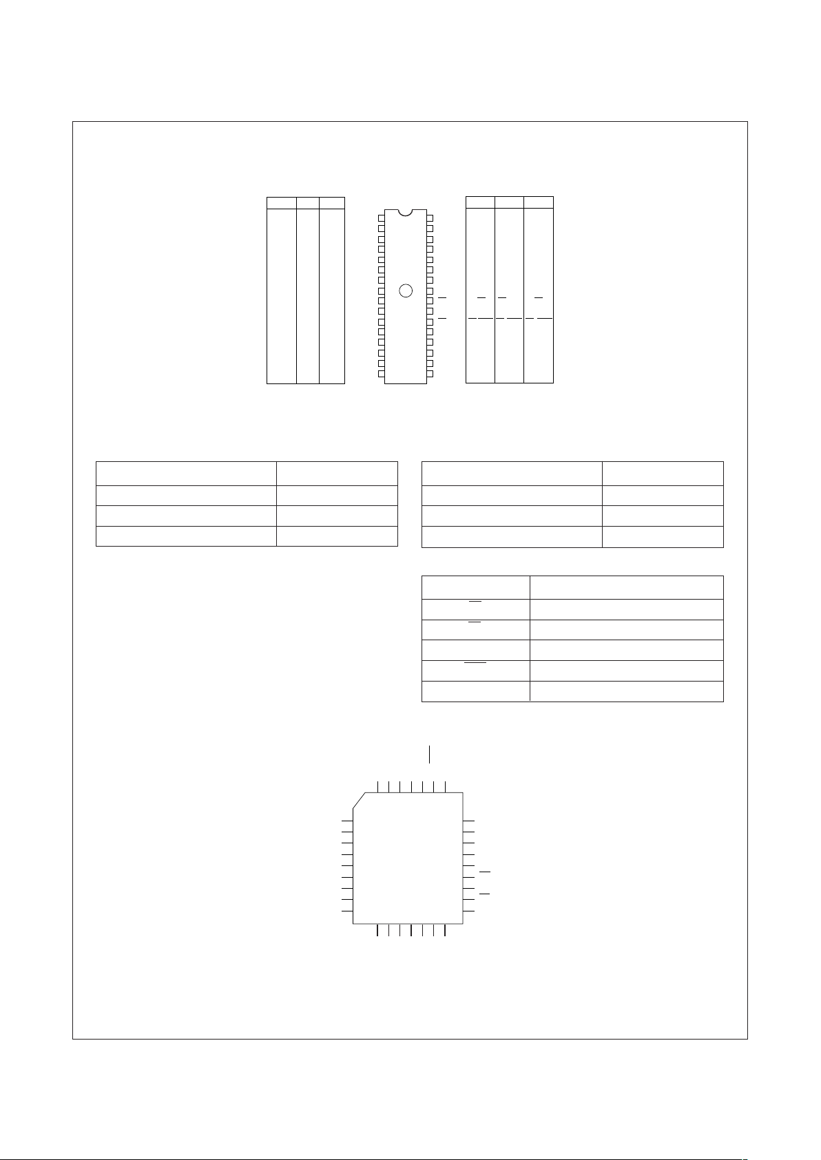
Connection Diagrams
DIP PIN CONFIGURATIONS
Note: Compatible EPROM pin configurations are shown in the blocks adjacent to the FM27C010 pins.
Commercial Temperature Range
(0°C to +70°C) VCC = 5V ±10%
Parameter/Order Number Access Time (ns)
FM27C010 Q, V, N 90 90
FM27C010 Q, V, N 120 120
FM27C010 Q, V, N 150 150
Extended Temperature Range
(-40°C to +85°C) VCC = 5V ±10%
Parameter/Order Number Access Time (ns)
FM27C010 QE, VE, NE 90 90
FM27C010 QE, VE, NE 120 120
FM27C010 QE, VE, NE 150 150
Package Types: FM27C010 Q, N, V XXX
Q = Quartz-Windowed Ceramic DIP package
V = PLCC package
N = Plastic DIP package
• All packages conform to JEDEC standard.
• All versions are guaranteed to function at slower speeds.
Pin Names
A0–A16 Addresses
CE Chip Enable
OE Output Enable
O0–O7 Outputs
PGM Program
XX Don’t Care (During Read)
PLCC Pin Configuration
Top View
DS800032-10
1
2
3
4
5
6
7
8
9
10
11
12
13
14
15
16
32
31
30
29
28
27
26
25
24
23
22
21
20
19
18
17
XX/V
PP
A
16
A
15
A
12
A
7
A
6
A
5
A
4
A
3
A
2
A
1
A
0
O
0
O
1
O
2
GND
XX/V
PP
A
16
A
15
A
12
A
7
A
6
A
5
A
4
A
3
A
2
A
1
A
0
O
0
O
1
O
2
GND
27C040
DIP
FM27C010
V
CC
XX/PGM
XX
A
14
A
13
A
8
A
9
A
11
OE
A
10
CE
O
7
O
6
O
5
O
4
O
3
V
PP
A
12
A
7
A
6
A
5
A
4
A
3
A
2
A
1
A
0
O
0
O
1
O
2
GND
27C256
A
15
A
12
A
7
A
6
A
5
A
4
A
3
A
2
A
1
A
0
O
0
O
1
O
2
GND
27C512
27C040
V
CC
A
18
A
17
A
14
A
13
A
8
A
9
A
11
OE
A
10
CE/PGM
O
7
O
6
O
5
O
4
O
3
V
CC
A
14
A
13
A
8
A
9
A
11
OE/V
PP
A
10
CE/PGM
O
7
O
6
O
5
O
4
O
3
V
CC
A
14
A
13
A
8
A
9
A
11
OE
A
10
CE/PGM
O
7
O
6
O
5
O
4
O
3
27C256 27C512
A
14
A
13
A
8
A
9
A
11
OE
A
10
CE
O
7
A
7
A
6
A
5
A
4
A
3
A
2
A
1
A
0
O
0
A12A15A16XX/VPPVCCXX/PGM
XX
O
1O2
GND
O
3O4O5O6
5
6
7
8
9
10
11
12
13
29
28
27
26
25
24
23
22
21
14 15 16 17 18 19 20
4 3 2 1 32 31 30
DS800032-3
3
www.fairchildsemi.com
FM27C010 1,048,576-Bit (128K x 8) High Performance CMOS EPROM
www.fairchildsemi.com
FM27C010
Absolute Maximum Ratings (Note 1)
Storage Temperature -65°C to +150°C
All Input Voltages Except A9 with
Respect to Ground (Note 10) -0.6V to +7V
VPP and A9 with Respect to Ground -0.6V to +14V
V
CC
Supply Voltage with
Respect to Ground -0.6V to +7V
ESD Protection >2000V
All Output Voltages with
Respect to Ground (Note 10) VCC + 1.0V to GND - 0.6V
Operating Range
Range Temperature V
CC
Tolerance
Commercial 0°C to +70°C +5V ±10%
Extended -40°C to +85°C +5V ±10%
DC Read Characteristics Over Operating Range with V
PP
= V
CC
Symbol Parameter Test Conditions Min Max Units
V
IL
Input Low Level -0.5 0.8 V
V
IH
Input High Level 2.0 VCC +1 V
V
OL
Output Low Voltage IOL = 2.1 mA 0.4 V
V
OH
Output High Voltage IOH = -2.5 mA 3.5 V
I
SB1
VCC Standby Current CE = VCC ± 0.3V 100 µA
(CMOS)
I
SB2
VCC Standby Current (TTL) CE = V
IH
1mA
I
CC
VCC Active Current CE = OE = V
IL
f = 5 MHz 30 mA
I/O = 0 mA
I
PP
VPP Supply Current VPP = V
CC
10 µA
V
PP
VPP Read Voltage VCC - 0.7 V
CC
V
I
LI
Input Load Current VIN = 5.5 or GND -1 1 µA
I
LO
Output Leakage Current V
OUT
= 5.5V or GND -10 10 µA
AC Read Characteristics Over Operating Range with V
PP
= V
CC
Symbol Parameter 70 90 120 150 Units
Min Max Min Max Min Max Min Max
t
ACC
Address to Output Delay 70 90 120 150
t
CE
CE to Output Delay 70 90 120 150
t
OE
OE to Output Delay 35 40 50 50
t
DF
Output Disable to Output 30 35 35 45 ns
(Note 2) Float
t
OH
Output Hold from
(Note 2) Addresses, CE or OE , 0 0 0 0
Whichever Occurred First
Capacitance T
A
= +25°C, f = 1 MHz (Note 2)
Symbol Parameter Conditions Typ Max Units
C
IN
Input Capacitance VIN = 0V 6 15 pF
C
OUT
Output Capacitance V
OUT
= 0V 10 15 pF
 Loading...