

Fairchild Semiconductor FDZ2554P Datasheet
July 2003
S
FDZ2554P
FDZ2554P
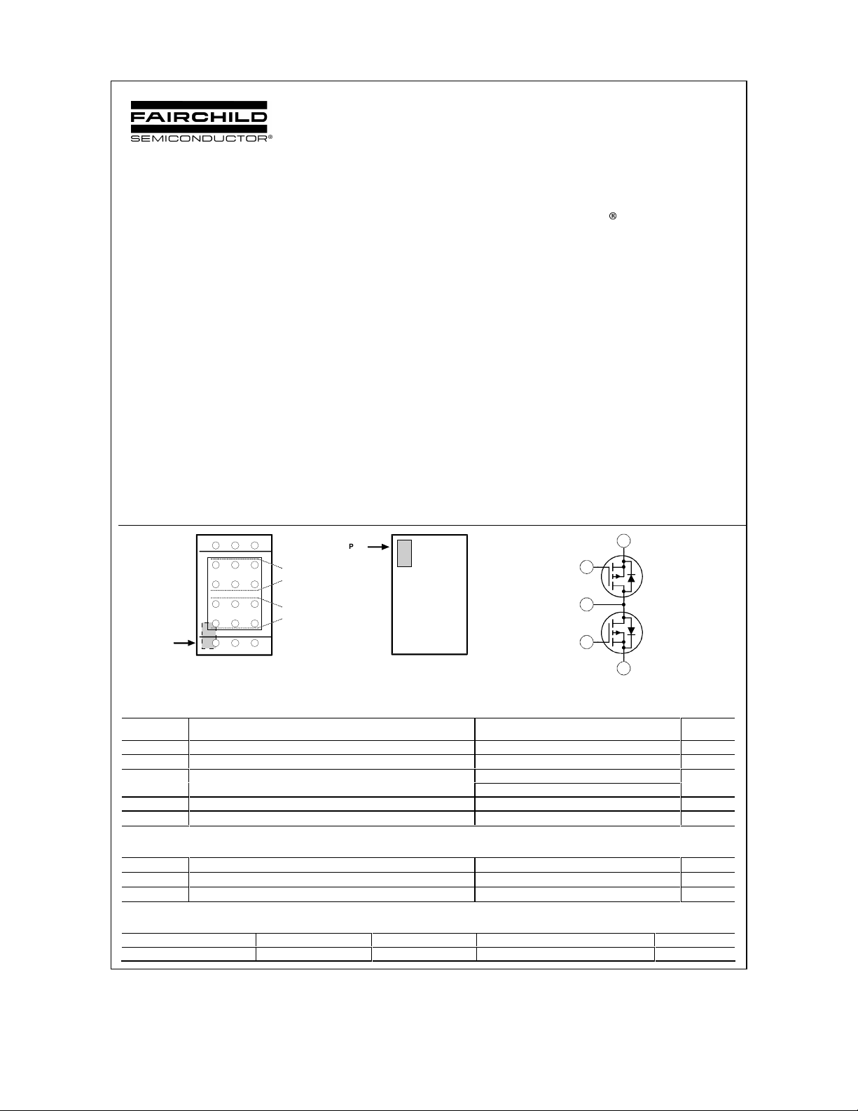
Monolithic Common Drain P-Channel 2.5V Specified PowerTrench BGA MOSFET
General Description
Combining Fairchild’s advanced 2.5V specified
PowerTrench process with state-of-the-art BGA
packaging, the FDZ2554P minimizes both PCB space
and R
. This monolithic common drain BGA
DS(ON)
MOSFET embodies a breakthrough in packaging
technology which enables the device to combine
excellent thermal transfer characteristics, high current
handling capability, ultra-low profile packaging, low gate
charge, and low R
DS(ON)
.
Applications
• Battery management
• Load switch
• Battery protection
D D
Pin 1
S
S
S
G
S
S
G
S S
D D D
D
S
Q2
S
S
Q1
Pin 1
Bottom
Top
Features
• –6.5 A, –20 V. R
R
• Occupies only 0.10 cm2 of PCB area:
1/3 the area of SO-8
• Ultra-thin package: less than 0.90 mm height when
mounted to PCB
• Outstanding thermal transfer characteristics:
significantly better than SO-8
• Ultra-low Qg x R
• High power and current handling capability
F255
4
= 28 mΩ @ VGS = –4.5 V
DS(ON)
= 45 mΩ @ VGS = –2.5 V
DS(ON)
figure-of-merit
DS(ON)
S
G
D
G
Q1
Q2
Absolute Maximum Ratings T
o
=25
C unless otherwise noted
A
Symbol Parameter Ratings Units
V
Drain-Source Voltage –20 V
DSS
V
Gate-Source Voltage ±12 V
GSS
ID Drain Current – Continuous (Note 1a) –6.5 A
– Pulsed –20
PD Power Dissipation (Steady State) (Note 1a) 2.1 W
TJ, T
Operating and Storage Junction Temperature Range –55 to +150 °C
STG
Thermal Characteristics
R
Thermal Resistance, Junction-to-Ambient (Note 1a) 60 °C/W
θJA
R
Thermal Resistance, Junction-to-Ambient (Note 1b) 108 °C/W
θJA
R
Thermal Resistance, Junction-to-Case (Note 1) 8 °C/W
θJC
Package Marking and Ordering Information
Device Marking Device Reel Size Tape width Quantity
2554P FDZ2554P 7’’ 12mm 3000 units
2003 Fairchild Semiconductor Corporation FDZ2554P Rev. C3 (W)
FDZ2554P
Electrical Characteristics T
= 25°C unless otherwise noted
A
Symbol Parameter Test Conditions Min Typ Max Units
Off Characteristics
BV
Drain–Source Breakdown Voltage VGS = 0 V, ID = –250 µA –20 V
DSS
∆BVDSS
∆TJ
I
Zero Gate Voltage Drain Current VDS = –16 V, VGS = 0 V –1 µA
DSS
I
Gate–Body Leakage VGS = ±12 V, VDS = 0 V ±100 nA
GSS
Breakdown Voltage Temperature
Coefficient
ID = –250 µA, Referenced to 25°C –13 mV/°C
On Characteristics (Note 2)
V
Gate Threshold Voltage VDS = VGS, ID = –250 µA –0.6 –0.8 –1.5 V
GS(th)
∆VGS(th)
∆TJ
R
DS(on)
I
On–State Drain Current VGS = –4.5 V, VDS = –5V –20 A
D(on)
Gate Threshold Voltage
Temperature Coefficient
Static Drain–Source
On–Resistance
ID = –250 µA, Referenced to 25°C
VGS = –4.5 V, ID = –6.5 A
VGS = –2.5 V, ID = –5 A
VGS = –4.5 V, ID = –6.5 A, TJ=125°C
3 mV/°C
21
36
30
28
45
43
mΩ
gFS Forward Transconductance VDS = –5 V, ID = –6.5 A 24 S
Dynamic Characteristics
C
Input Capacitance 1430
iss
C
Output Capacitance 319 pF
oss
C
Reverse Transfer Capacitance
rss
VDS = –10 V, V
f = 1.0 MHz
= 0 V,
GS
164 pF
RG Gate Resistance VGS = 15 mV, f = 1.0 MHz 9.2
pF
Ω
Switching Characteristics (Note 2)
t
Turn–On Delay Time 12 22 ns
d(on)
tr Turn–On Rise Time 9 18 ns
t
Turn–Off Delay Time 62 100 ns
d(off)
tf Turn–Off Fall Time
Qg Total Gate Charge 14 20 nC
Qgs Gate–Source Charge 3 nC
Qgd Gate–Drain Charge
VDD = –10 V, ID = –1 A,
VGS = –4.5 V, R
GEN
= 6 Ω
VDS = –10 V, ID = –6.5 A,
VGS = –4.5 V
37 60 ns
4 nC
Drain–Source Diode Characteristics and Maximum Ratings
IS Maximum Continuous Drain–Source Diode Forward Current –1.75 A
VSD Drain–Source Diode Forward
Voltage
trr Reverse Recovery Time
Qrr Reverse Recovery Charge
Notes: 1. R
Scale 1 : 1 on letter size paper
2. Pulse Test: Pulse Width < 300µs, Duty Cycle < 2.0%
is determined with the device mounted on a 1 in² 2 oz. copper pad on a 1.5 x 1.5 in. board of FR-4 material. The thermal resistance from the
θJA
junction to the circuit board side of the solder ball, R
top surface of the copper chip carrier. R
θJC
a) 60°C/W when mounted
on a 1in2 pad of 2 oz
copper
VGS = 0 V, IS = –1.75 A (Note 2) –0.7 –1.2 V
IF = –6.5 A,
diF/dt = 100 A/µs
, is defined for reference. For R
θJB
and R
are guaranteed by design while R
θJB
, the thermal reference point for the case is defined as the
θJC
is determined by the user's board design.
θJA
25
20 nC
b) 108°C/W when mounted
on a minimum pad of 2 oz
copper
ns
FDZ2554P Rev C3 (W)
 Loading...