

Fairchild Semiconductor FDS8433A Datasheet
FDS8433A
Single P-Channel 2.5V Specified MOSFET
FDS8433A
October 1998
PRELIMINARY
General Description
This P-Channel enhancement mode power field effect
transistors is produced using Fairchild’s proprietary,
high cell density, DMOS technology. This very high
density processis especially tailored to minimize
on-state resistance and provide superior switching
performance.
Applications
• Load switch
• DC/DC converter
• Battery protection
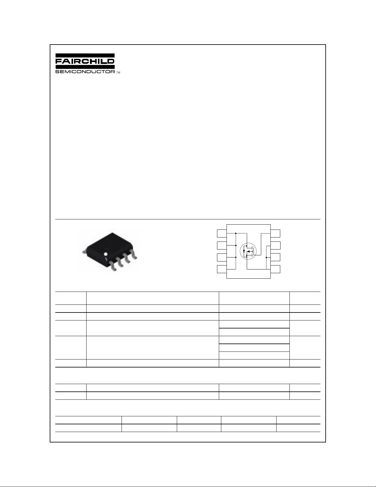
D
D
D
D
G
S
SO-8
Absolute Maximum Ratings
S
S
TA = 25°C unless otherwise noted
Features
• -5 A, -20 V. R
R
= 0.045 Ω @ V
DS(on)
= 0.070 Ω @ V
DS(on)
= -4.5 V
GS
= -2.5 V
GS
• Fast switching speed.
• High density cell design for extremely low R
• High power and current handling capability.
5
6
7
8
4
3
2
1
DS(on)
.
Symbol Parameter FDS8433A Units
V
DSS
V
GSS
I
D
P
D
TJ, T
stg
Drain-Source Voltage -20 V
Gate-Source Voltage
Drain Current - Continuous
- Pulsed -50
Power Dissipation for Si ngl e Operat i on
Operating and Storage Junction Temperature Range -55 to +150
(Note 1a)
(Note 1a)
(Note 1b)
(Note 1c)
8V
±
-5 A
2.5 W
1.2
1
Thermal Characteristics
R
JA
θ
R
JC
θ
Thermal Resistance, J unc tion-to-Ambient
Thermal Resistance, J unc tion-to-Case
(Note 1a)
(Note 1)
50
25
Package Outlines and Ordering Information
Device Marking Device Reel Size Tape Width Quantity
FDS8433A FDS8433A 13’’ 12mm 2500 units
1998 Fairchild Semiconductor Corporation
C
°
C/W
°
C/W
°
FDS8433A Rev. B1
FDS8433A
yp
DMOS Electrical Characteristics
TA = 25°C unless otherwise noted
Symbol Parameter Test Conditions Min T
Off Characteristics
BV
DSS
DSS
BV
T
∆
I
DSS
I
GSSF
I
GSSR
On Characteristics
V
GS(th)
GS(th)
V
∆
T
∆
R
DS(on)
I
D(on)
g
FS
Drain-Source Breakdown Voltage VGS = 0 V, ID = -250 µA-20 V
Breakdown Voltage Temperature
Coefficient
J
ID = -250 µA, Referenced to 25°C-25 mV/
Zero Gate Voltage Drain Current VDS = -16 V, VGS = 0 V -1
Gate-Body Leakage Current, Forward VGS = 8 V, VDS = 0 V 100 nA
Gate-Body Leakage Current, Reverse VGS = -8 V, VDS = 0 V -100 nA
(Note 2)
Gate Threshold Voltage VDS = VGS, ID = -250 µA -0.4 -0.6 -1 V
Gate Threshold Voltage
Temperature Coefficient
J
Static Drain-Source
On-Resistance
ID = -250 µA, Referenced to 25°C4 mV/
VGS = -4.5 V, ID = -5 A
V
= -4.5 V, ID = -5 A, TJ=125°C
GS
V
= -2.5 V, ID = -4.3 A
GS
On-State Drain Current VGS = -4.5 V, VDS = -5 V -25 A
Forward Transconductance VDS = -5 V, ID = -5 A 16 S
Dynamic Characteristics
C
iss
C
oss
C
rss
Input Capacitance 1130 pF
Output Capacitance 480 pF
= -10 V, VGS = 0 V,
V
DS
f = 1.0 MHz
Reverse Transfer Capacitance
Max Units
0.045
0.036
0.085
0.050
0.070
0.047
120 pF
C
°
A
µ
C
°
Ω
Ω
Ω
(Note 2)
Switching Characteristics
t
t
t
t
Q
Q
Q
d(on)
r
d(off)
f
g
gs
gd
Turn-On Delay Time 8 16 ns
Turn-On Rise Time 23 37 ns
Turn-Off Delay Time 260 360 ns
Turn-Off Fall Time
Total Gate Charge 20 28 nC
Gate-Source Charge 2.8 nC
Gate-Drain Charge
V
= -10 V, ID = -1 A,
DD
V
= -4.5 V, R
GS
= -5 V, ID = -5 A,
V
DS
V
= -5 V,
GS
GEN
= 6
Ω
90 125 ns
3.2 nC
Drain-Source Diode Characteristics and Maximum Ratings
I
S
V
SD
Notes:
1: R
θJA
drain pins. R
Scale 1 : 1 on letter size paper
2: Pulse Test: Pulse Width ≤ 300 µs, Duty Cycle ≤ 2.0%
Maximum Continuous Drain-Source Diode Forward Current -2.1 A
Drain-Source Diode Forward Voltage VGS = 0 V, IS = -2.1 A
is the sum of the junction-to-case and case-to-ambient resistance where the case thermal reference is defined as the solder mounting surface of the
is guaranteed by design while R
θJC
a) 50° C/W when
mounted on a 1 in
pad of 2 oz. copper.
is determined by the user's board design.
θJA
2
b) 105° C/W when
mounted on a 0.04 in
pad of 2 oz. copper.
(Note 2)
2
-0.8 -1.2 V
c) 125° C/W when mounted
on a 0.006 in2 pad
of 2 oz. copper.
FDS8433A Rev. B1
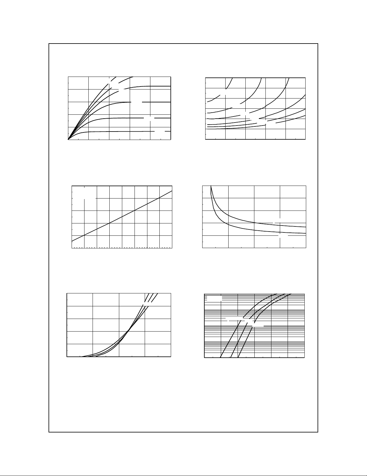
T ypical Characteristics
FDS8433A
50
40
30
20
10
D
- I , DRAIN-SOURCE CURRENT (A)
0
012345
V = -4.5V
GS
-3.5V
-3.0V
-2.5V
-V , DRAIN-SOURCE VOLTAGE (V)
DS
-2.0V
-1.5V
2
1.8
V = -2 .0V
GS
1.6
1.4
1.2
DS( o n)
R , NOR MA LIZ ED
1
DRAIN-SO URCE ON-RESI STAN CE
0.8
0 1020304050
-2.5V
-3.0V
-3.5V
-4.0V
- I , DRAIN CURRENT (A)
D
Figure 1. On-Region Characteristics. Figure 2. On-Resistance Variation
with Drain Current and Gate V oltage.
1.6
I = -5A
D
V = -4.5V
GS
1.4
1.2
1
DS(ON)
R , NORMALIZED
0.8
DRAIN-SOURCE ON-RESISTANCE
0.6
-50 -25 0 25 50 75 100 125 150
T , JUNCTION TEMPERATURE (°C)
J
0.15
0.12
0.09
0.06
0.03
DS(ON)
R , ON-R E SISTA N CE (OHM)
0
12345
-V , GATE TO S OURCE VOLT AG E ( V)
GS
-4.5V
T = 125°C
J
I = -2.5A
D
25° C
Figure 3. On-Resistance Variation
with Temperature.
10
V = -5V
DS
8
6
4
D
- I , DRAIN CURRENT ( A)
2
0
0.4 0.8 1.2 1.6 2
-V , GA TE TO SOURCE V OLTAGE (V)
GS
T = -55 °C
J
25°C
125°C
Figure 5. Transfer Characteristics.
Figure 4. On-Resistance Variation
with Gate-to-Source Voltage.
10
V = 0V
GS
3
1
T =1 25° C
J
25°C
0.1
0.01
S
- I , REVERS E DRAI N CURRENT (A)
0.001
0 0.2 0.4 0.6 0. 8 1 1.2
-V , BODY DI ODE FORWARD VOLT AGE (V)
SD
-55°C
Figure 6. Body Diode Forward Voltage
Variation with Source Current
and Temperature.
FDS8433A Rev. B1
 Loading...