

Fairchild Semiconductor FDS8333C Datasheet
August 2002
G
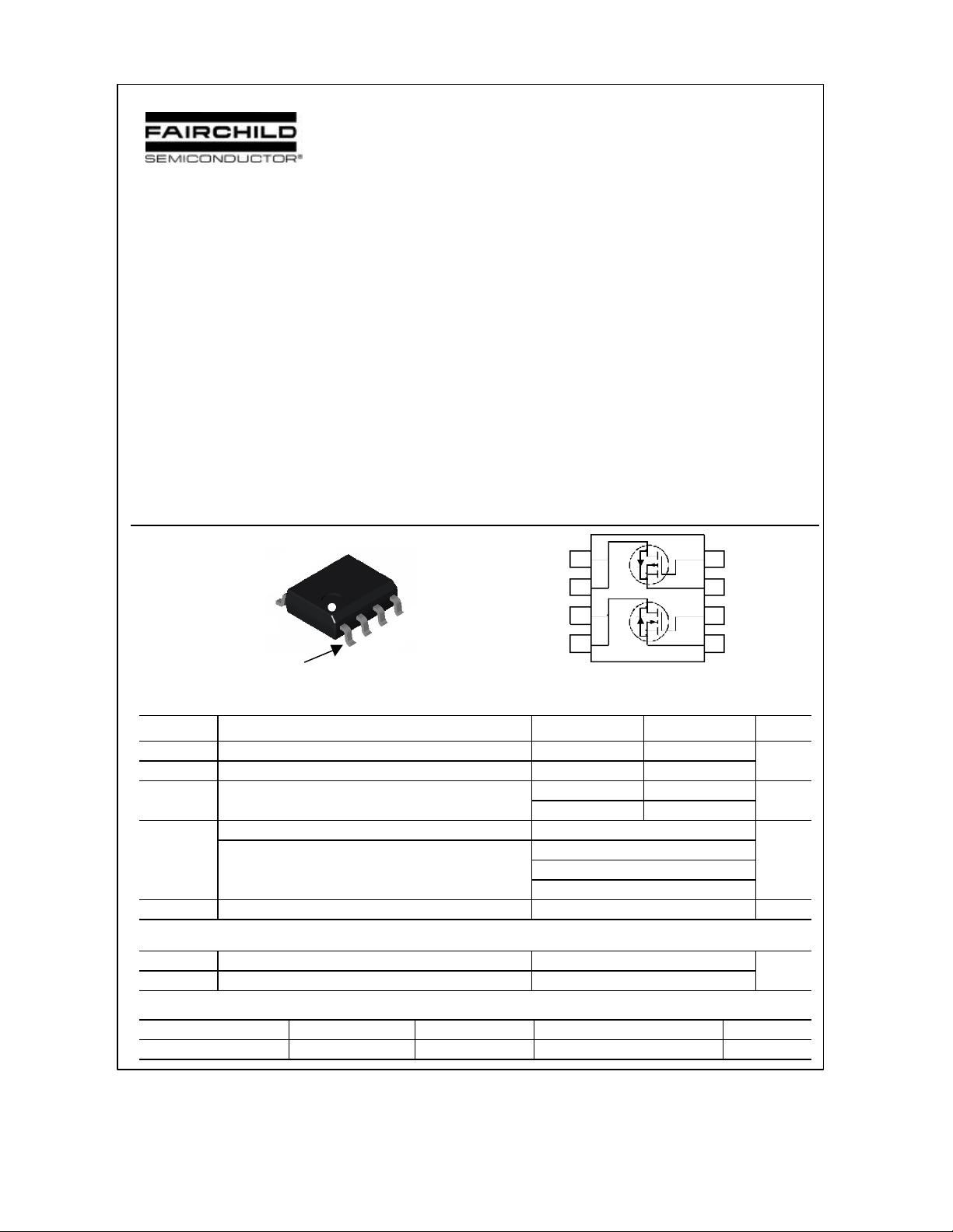
FDS8333C
FDS8333C
30V N & P-Channel PowerTrench MOSFETs
General Description
These N & P-Channel MOSFETs are
produced using Fairchild Semiconductor’s
advanced PowerTrench process that has been
especially tailored to minimize on-state
resistance and yet maintain superior switching
performance.
These devices are well suited for low voltage
and battery powered applications where low
in-line power loss and fast switching are
required.
D2
D
D2
D
D1
D
D1
D
SO-8
Pin 1
SO-8
S1
S2
G1
S
S
S
Absolute Maximum Ratings T
G2
=25
A
Features
• Q1 4.1 A, 30V. R
R
• Q2 –3.4 A, 30V. R
R
• Low gate charge
• High performance trench technology for extremely
low R
• High power and handling capability in a widely used
surface mount package.
o
C unless otherwise noted
DS(ON)
= 80 mΩ @ VGS = 10 V
DS(ON)
= 130 mΩ @ VGS = 4.5 V
DS(ON)
= 130 mΩ @ VGS = –10 V
DS(ON)
= 200 mΩ @ VGS = –4.5 V
DS(ON)
.
Q2
5
6
Q1
7
8
4
3
2
1
Symbol Parameter Q1 Q2 Units
V
Drain-Source Voltage 30 –30 V
DSS
V
Gate-Source Voltage ±16 ±20
GSS
ID Drain Current – Continuous (Note 1a) 4.1 –3.4 A
– Pulsed 20 –20
PD
TJ, T
STG
Power Dissipation for Dual Operation 2
Power Dissipation for Single Operation (Note 1a)
(Note 1b) 1
(Note 1c) 0.9
Operating and Storage Junction Temperature Range –55 to +150 °C
1.6
W
Thermal Characteristics
R
Thermal Resistance, Junction-to-Ambient (Note 1a)
θJA
R
Thermal Resistance, Junction-to-Case (Note 1)
θJC
78
40
°C/W
Package Marking and Ordering Information
Device Marking Device Reel Size Tape width Quantity
FDS8333C FDS8333C 7’’ 12mm 2500 units
2002 Fairchild Semiconductor Corporation FDS8333C Rev C (W)
Q1
FDS8333C
Electrical Characteristics T
Symbol
Off Characteristics
BV
Drain–Source Breakdown Voltage
DSS
∆BVDSS
∆TJ
I
Zero Gate Voltage Drain Current
DSS
I
GSSF
I
GSSF
Breakdown Voltage Temperature
Coefficient
/I
Gate–Body Leakage, Forward
GSSR
/I
Gate–Body Leakage, Reverse
GSSR
On Characteristics (Note 2)
V
GS(th)
∆VGS(th)
∆TJ
R
DS(on)
I
D(on)
gFS Q1
Gate Threshold Voltage
Gate Threshold Voltage
Temperature Coefficient
Q1
Static Drain–Source
On–Resistance
Q1
On–State Drain Current
Forward Transconductance
Parameter Test Conditions Min Typ Max Units
Q1
Q2
Q2
Q2
Q2
= 25°C unless otherwise noted
A
Q1
VGS = 0 V, ID = 250 µA
VGS = 0 V, ID = –250 µA
ID = 250 µA,Ref. to 25°C
ID = –250 µA,Ref. to 25°C
VDS = 24 V, VGS = 0 V
VDS = –24 V, VGS = 0 V
VGS = ± 16 V, VDS = 0 V
VGS = ± 20V , VDS = 0 V
Q2
Q1
Q2
Q2
30
–30
V
25
–22
1
–1
±100
±100
VDS = VGS, ID = 250 µA 1 1.7 3
VDS = VGS, ID = –250 µA –1 –1.8 –3
ID = 250 µA,Ref. To 25°C Q1
ID = –250 µA,Ref. to 25°C Q2
VGS = 10 V, ID = 4.1 A
VGS = 4.5 V, ID = 3.2 A
VGS = 10 V, ID = 4.1 A TJ=125°C
VGS = –10 V, ID = –3.4 A
VGS = – 4.5 V, ID = –2.5 A
VGS = –10V,ID = –3.4A, TJ=125°C
VGS = 10 V, VDS = 5 V
VGS = –10 V, VDS = –5 V
VDS = 5 V ID = 4.1 A
VDS = –5 V ID = –3.4A
–4.2
3.7
67
130
81
145
103
105
167
147
130
200
220
10
–5
9
5
80
mV/°C
µA
nA
nA
V
mV/°C
m Ω
A
S
Dynamic Characteristics
C
Q1
iss
C
oss
C
Q1
rss
RG Q1
Input Capacitance
Q2
Q1
Output Capacitance
Q2
Reverse Transfer Capacitance
Q2
Gate Resistance
Q2
Switching Characteristics (Note 2)
t
Q1
d(on)
tr Q1
t
d(off)
tf Q1
Qg Q1
Qgs Q1
Qgd Q1
Turn–On Delay Time
Q2
Turn–On Rise Time
Q2
Q1
Turn–Off Delay Time
Q2
Turn–Off Fall Time
Q2
Total Gate Charge
Q2
Gate–Source Charge
Q2
Gate–Drain Charge
Q2
VDS=10 V, V
VDS=–10 V, V
VDS=10 V, V
VDS=–10 V, V
VDS=10 V, V
VDS=–10 V, V
= 0 V, f=1.0MHz 282
GS
= 0 V, f=1.0MHz
GS
= 0 V, f=1.0MHz
GS
= 0 V, f=1.0MHz
GS
= 0 V, f=1.0MHz
GS
= 0 V, f=1.0MHz
GS
VGS= 15 mV, f=1.0MHz
VGS=–15 mV, f=1.0MHz
For Q1:
V
=10 V, I
DS
VGS= 4.5 V, R
DS
GEN
= 1 A
= 6 Ω
For Q2:
V
=–10 V, I
DS
VGS= –4.5 V, R
= –1 A
DS
GEN
= 6 Ω
For Q1:
V
=10 V, I
DS
VGS= 4.5 V, R
= 4.1 A
DS
GEN
= 6 Ω
For Q2:
V
=–10 V, I
DS
= –3.4 A
DS
VGS= –4.5 V,
185
49
56
20
26
2.3
–9.6
4.5 9
4.5 9
6 12
13 23
19 34
11 20
1.5 3
2 4
4.7 6.6
4.1 5.7
0.9
0.8
0.6
0.4
pF
pF
pF
Ω
ns
ns
ns
ns
nC
nC
nC
FDS8333C Rev C (W)
FDS8333C
Electrical Characteristics T
Symbol
Parameter Test Conditions Min Typ Max Units
= 25°C unless otherwise noted
A
Drain–Source Diode Characteristics and Maximum Ratings
VSD Q1
trr Q1
Qrr Q1
Notes:
1. R
θJA
the drain pins. R
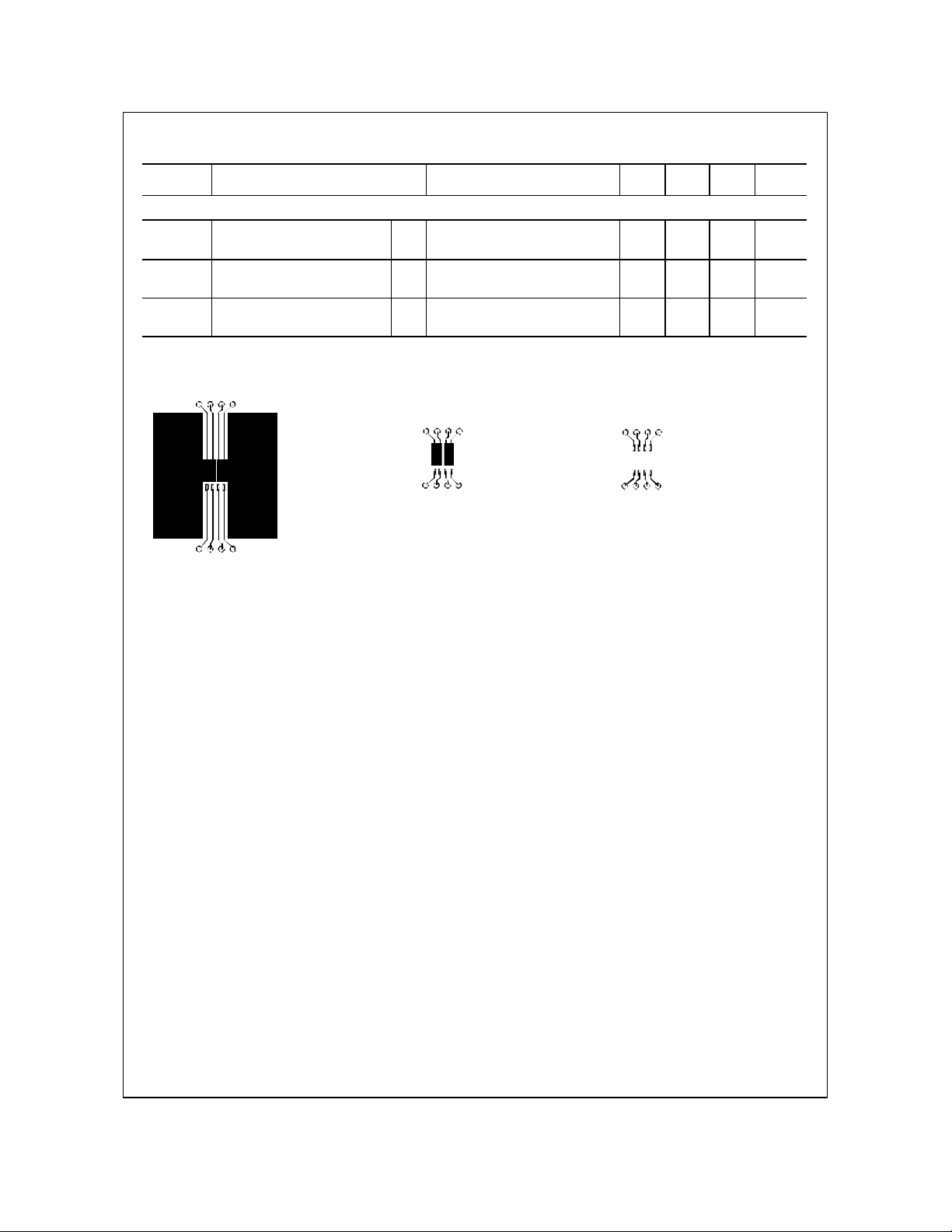
Scale 1 : 1 on letter size paper
2. Pulse Test: Pulse Width < 300µs, Duty Cycle < 2.0%
Drain–Source Diode Forward
Voltage
Diode Reverse Recovery
Time
Diode Reverse Recovery
Charge
is the sum of the junction-to-case and case-to-ambient thermal resistance where the case thermal reference is defined as the solder mounting surface of
is guaranteed by design while R
θJC
a) 78°C/W when
θCA
mounted on a
0.5in2 pad of 2
oz copper
is determined by the user's board design.
VGS = 0 V, IS = 1.3 A (Note 2)
VGS = 0 V, IS = –1.3 A (Note 2)
Q2
IF = 4.1 A, diF/dt = 100 A/µs
IF = –3.4 A, diF/dt = 100 A/µs
Q2
IF = 4.1 A, diF/dt = 100 A/µs
IF = –3.4 A, diF/dt = 100 A/µs
Q2
b) 125°C/W when
mounted on a
0.02 in2 pad of
2 oz copper
0.8 1.2
0.8 –1.2
16.3
14.5
26.7
21.1
c) 135°C/W when
mounted on a
minimum pad.
V
nS
nC
FDS8333C Rev C (W)
 Loading...