

Fairchild Semiconductor FDS7760A Datasheet
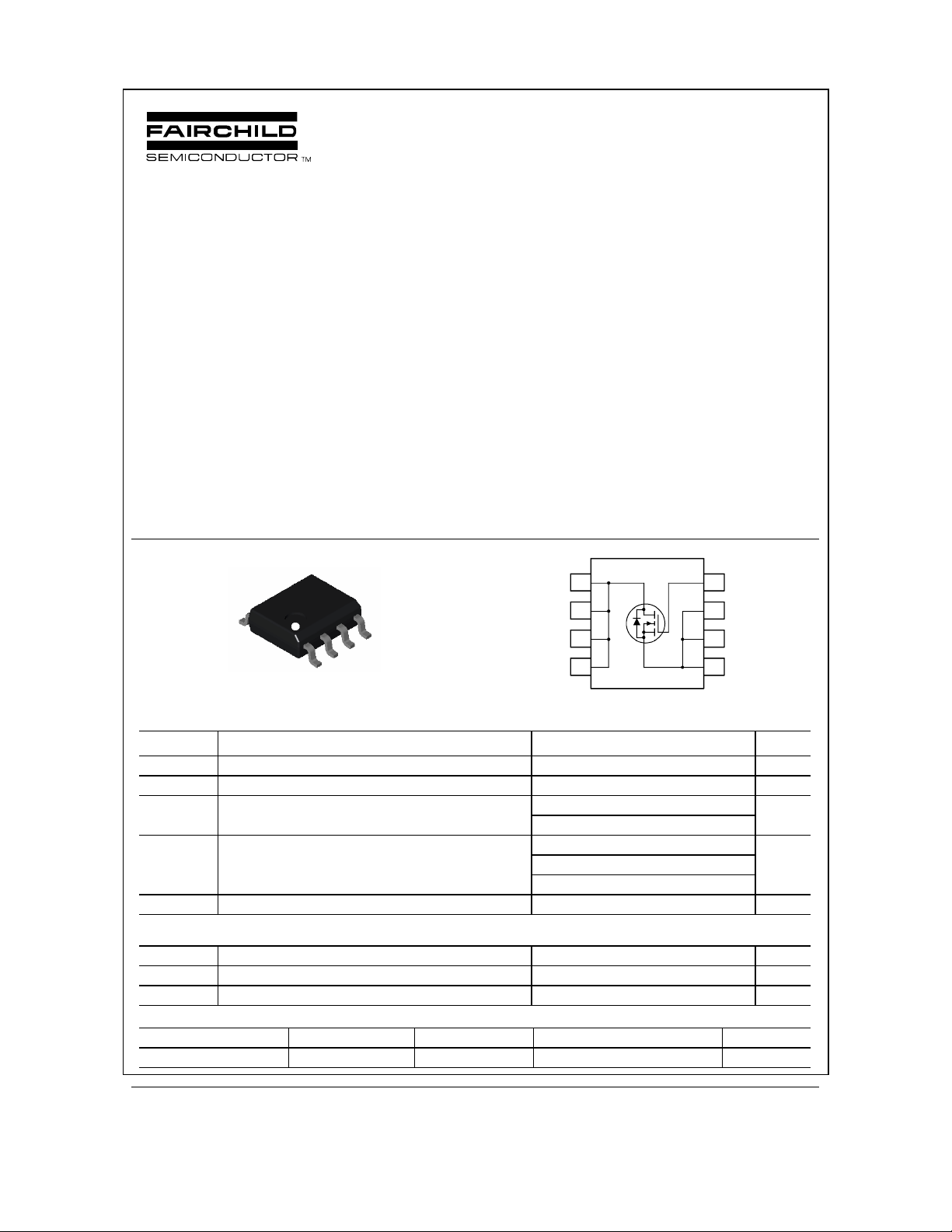
FDS7760A
N-Channel Logic Level PowerTrench® MOSFET
FDS7760A
February 2000
PRELIMINARY
General Description
This N-Channel Logic Level MOSFET is produced
using Fairchild Semiconductor’s advanced
PowerTrench process that has been especially tailored
to minimize on-state resistance and yet maintain
superior switching performance.
These devices are well suited for low voltage and
Features
15 A, 30 V. R
•
Low gate charge (37nC typical)
•
Fast switching speed.
•
= 5.5 mΩ @ VGS = 10 V
DS(ON)
R
= 8 mΩ @ VGS = 4.5 V.
DS(ON)
battery powered applications where low in-line power
loss and fast switching are required.
Applications
DC/DC converter
•
Load switch
•
Motor drives
•
D
D
D
D
S
SO-8
S
S
Absolute Maximum Ratings
G
TA=25oC unless otherwise noted
High performance trench technology for extremely
•
DS(ON)
.
5
6
7
8
4
3
2
1
low R
High power and current handling capability.
•
Symbol Parameter Ratings Units
V
DSS
V
GSS
I
D
P
D
TJ, T
STG
Drain-Source Voltage 30 V
Gate-Source Voltage
Drain Current – Continuous
(Note 1a)
20
±
15 A
– Pulsed 60
Power Dissipation for Single Operation
(Note 1a)
(Note 1b)
(Note 1c)
2.5
1.2
1
Operating and Storage Junction Temperature Range -55 to +150
V
W
C
°
Thermal Characteristics
R
JA
θ
R
JA
θ
R
JC
θ
Thermal Resistance, Junction-to-Ambient
Thermal Resistance, Junction-to-Ambient
Thermal Resistance, Junction-to-Case
(Note 1a)
(Note 1c)
(Note 1)
50
50 (10 sec)
30
Package Outlines and Ordering Information
Device Marking Device Reel Size Tape Width Quantity
FDS7760A FDS7760A 13’’ 12mm 2500 units
1999 Fairchild Semiconductor Corpor ation
C/W
°
C/W
°
C/W
°
FDS7760A Rev. B (W)
FDS7760A
DMOS Electrical Characteristics
TA = 25°C unless otherwise noted
Symbol Parameter Test Conditions Min Typ Max Units
Off Characteristics
BV
DSS
BV
∆
T
∆
I
DSS
I
GSSF
I
GSSR
On Characteristics
V
GS(th)
GS(th)
V
∆
T
∆
R
DS(on)
I
D(on)
g
FS
Drain–Source Breakdown Voltage
Breakdown Voltage Temperature
DSS
Coefficient
J
V
= 0 V, ID = 250 µA
GS
I
= 250 µA, Referenced to 25°C
D
30 V
24
Zero Gate Voltage Drain Current VDS = 24 V, VGS = 0 V 1
Gate–Body Leakage, Forward VGS = 20 V, VDS = 0 V 100 nA
Gate–Body Leakage, Reverse VGS = –20 V VDS = 0 V –100 nA
(Note 2)
Gate Threshold Voltage
Gate Threshold Voltage
Temperature Coefficient
J
Static Drain–Source
On–Resistance
V
= VGS, ID = 250 µA
DS
I
= 250 µA, Referenced to 25°C
D
VGS = 10 V, ID = 15 A
= 10 V, ID = 15 A, TJ = 125°C
V
GS
= 4.5 V, ID = 13 A
V
GS
11.63 V
-5
4.5
7
6
On–State Drain Current VGS = 10 V, VDS = 5 V 50 A
Forward Transconductance VDS = 10 V, ID = 15 A 65 S
5.5
10
mV/°C
A
µ
mV/°C
m
Ω
8
Dynamic Characteristics
C
iss
C
oss
C
rss
Switching Characteristics
t
d(on)
t
r
t
d(off)
t
f
Q
g
Q
gs
Q
gd
Input Capacitance 3514 pF
Output Capacitance 1123 pF
Reverse Transfer Capacitance
(Note 2)
Turn–On Delay Time 13 20 ns
Turn–On Rise Time 12 19 ns
= 15 V, V
V
DS
f = 1.0 MHz
V
= 15 V, ID = 1 A,
DD
= 10 V, R
V
GS
GS
GEN
= 0 V,
= 6
307 pF
Ω
Turn–Off Delay Time 78 125 ns
Turn–Off Fall Time
Total Gate Charge 37 55 nC
Gate–Source Charge 10 nC
V
= 15 V, ID = 15 A,
DS
V
= 5 V
GS
Gate–Drain Charge
32 51 ns
12 nC
Drain–Source Diode Characteristics and Maximum Ratings
I
S
V
SD
Notes:
R
is the sum of the junction-to-case and case-to-ambient thermal resistance where the case thermal reference is defined as the solder mounting surface of
1.
JA
θ
the drain pins. R
Scale 1 : 1 on letter size paper
Pulse Test: Pulse Width < 300µs, Duty Cycle < 2.0%
2.
Maximum Continuous Drain–Source Diode Forward Current 2.1 A
Drain–Source Diode Forward
VGS = 0 V, IS = 2.1 A
(Note 2)
0.7 1.2 V
Voltage
is guaranteed by design while R
JC
θ
a) 50°/W when
mounted on a 1in
pad of 2 oz copper
is determined by the user's board design.
CA
θ
2
b) 105°/W when
mounted on a .04 in
pad of 2 oz copper
2
c) 125°/W when mounted on a
minimum pad.
FDS7760A Rev. B (W)
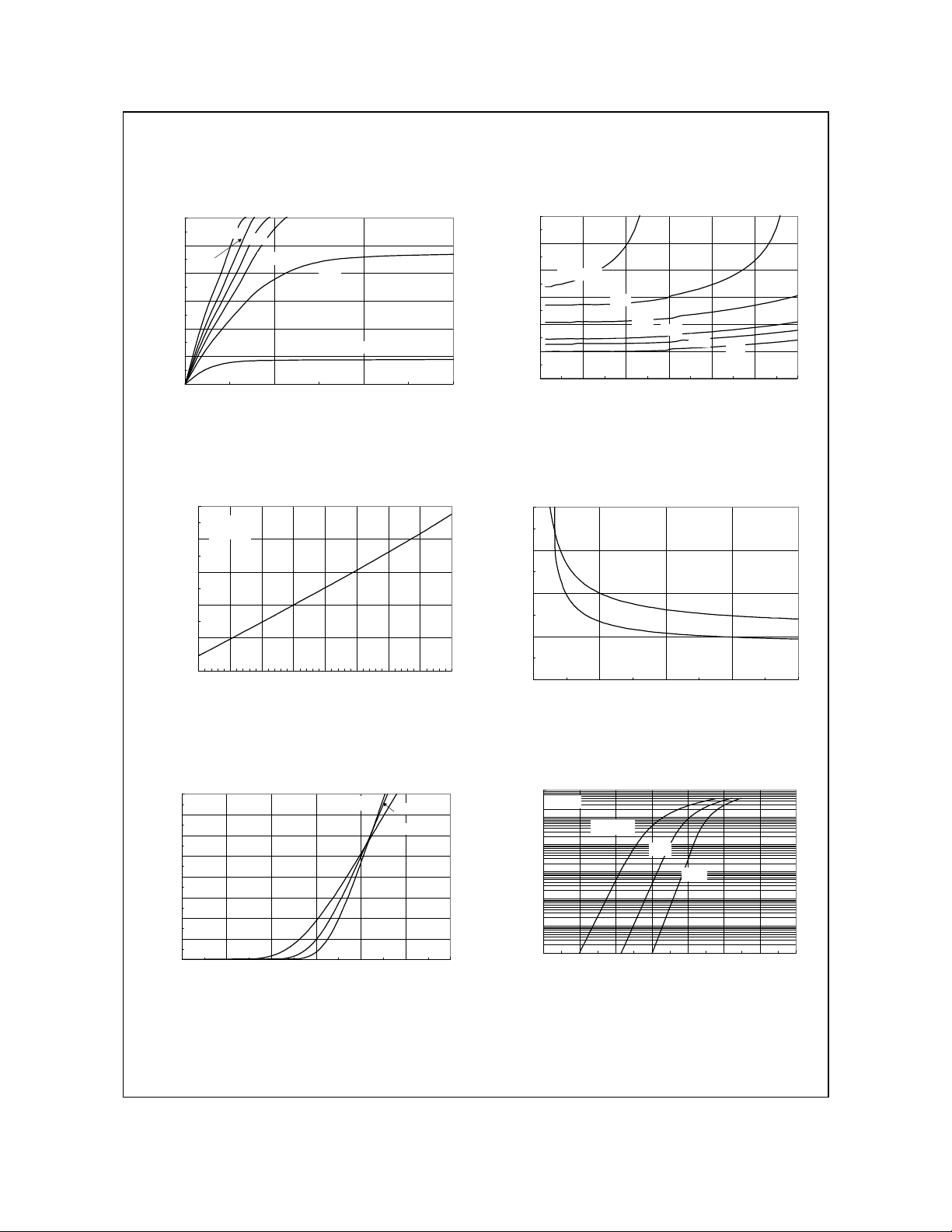
Typical Characteristics
FDS7760A
60
VGS = 10V
50
5.0
40
30
20
, DRAIN CURRENT (A)
D
I
10
0
00.511.5
4.0V
3.5V
V
, DRAIN-SOURCE VOLTAGE (V)
DS
3.0V
2.5V
2
1.8
1.6
VGS = 4.0V
1.4
, NORMALIZED
1.2
DS(ON)
R
1
DRAIN-SOURCE ON-RESISTANCE
0.8
0 102030405060
4.5V
5.0V
6.0V
, DRAIN CURRENT (A)
I
D
7.0V
Figure 1. On-Region Characteristics. Figure 2. On-Resistance Variation with
Drain Current and Gate Voltage.
1.6
ID = 9A
V
= 10V
GS
1.4
1.2
, NORMALIZED
1
DS(ON)
R
0.8
DRAIN-SOURCE ON-RESISTANCE
0.6
-50 -25 0 25 50 75 100 125 150
, JUNCTION TEMPERATURE (oC)
T
J
0.02
0.015
0.01
, ON-RESISTANCE (OHM)
0.005
DS(ON)
R
0
246810
, GATE TO SOURCE VOLTAGE (V)
V
GS
TA = 125oC
TA = 25oC
10V
ID = 7.5 A
Figure 3. On-Resistance Variation with
Temperature.
80
VDS = 5V
70
60
50
40
30
, DRAIN CURRENT (A)
20
D
I
10
0
11.522.533.54
V
, GATE TO SOURCE VOLTAGE (V)
GS
TA = -55oC
25oC
125oC
Figure 4. On-Resistance Variation with
Gate-to-Source Voltage.
100
VGS = 0V
10
1
0.1
0.01
0.001
, REVERSE DRAIN CURRENT (A)
S
I
0.0001
0 0.2 0.4 0.6 0.8 1 1.2 1.4
TA = 125oC
25oC
-55oC
, BODY DIODE FORWARD VOLTAGE (V)
V
SD
Figure 5. Transfer Characteristics. Figure 6. Body Diode Forward Voltage Variation
with Source Current and Temperature.
FDS7760A Rev. B (W)
 Loading...