Fairchild Semiconductor FDS6982 Datasheet

FDS6982
(
)
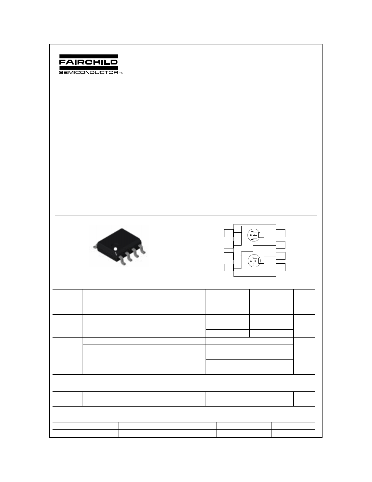
Dual N-Channel, Notebook Power Supply MOSFET
General Description
This part is designed to replace two single SO-8 MOSFET s
in synchronous DC:DC power supplies that provide the
various peripheral voltage rails required in notebook
computers and other battery powered electronic devices.
FDS6982 contains two unique 30V, N-channel, logic level,
PowerTrenchTM MOSFETs designed to maximize power
conversion efficiency.
The high-side switch (Q1) is designed with specific
emphasis on reducing switching losses while the low-side
switch (Q2) is optimized for low conduction (less than 20mΩ
at VGS = 4.5V).
Applications
• Battery powered synchronous DC:DC converters.
• Embedded DC:DC conversion.
Features
• Q2: 8.6A, 30V. R
R
• Q1: 6.3A, 30V. R
R
• Fast switching speed.
• Low gate charge (Q1 typical = 8.5nC).
• High performance trench technology for extremely
low R
DS(ON)
.
= 0.015 Ω @ V
DS(on)
= 0.020 Ω @ V
DS(on)
= 0.028 Ω @ V
DS(on)
= 0.035 Ω @ V
DS(on)
June 1999
= 10V
GS
= 4.5V
GS
= 10V
GS
= 4.5V
GS
FDS6982
D2
D2
D1
D1
G2
S2
SO-8
G1
S1
Absolute Maximum Ratings
Symbol Parameter
V
DSS
V
GSS
I
D
P
D
TJ, T
stg
Drain-Source Voltage 30 30 V
Gate-Source Voltage
Drain Current - Continuous
- Pulsed 30 20
Power Dissipation for Dual Operation 2 W
Power Dissipation for Single Operation
Operating and Storage Junction Temperature Range -55 to +150
Thermal Characteristics
R
JA
θ
R
JC
θ
Thermal Resistance, Junction-to-Ambient
Thermal Resistance, Junction-to-Case
TA = 25°C unless otherwise noted
(Note 1a)
Note 1a
(Note 1b)
(Note 1c)
(Note 1a)
(Note 1)
5
Q1
6
7
Q2
8
Q2
20
±
8.6 6.3 A
1.6
1
0.9
78
40
4
3
2
1
Q1
20 V
±
Units
°
°
C
°
C/W
C/W
Package Marking and Ordering Information
Device M a rk in g Device Ree l S iz e Tape W id th Quantity
FDS6982 FDS6982 13” 12mm 2500 units
1999 Fairchild Semiconductor Corporation
FDS6982, Rev. C

FDS6982
Electrical Characteristics
TA = 25°C unless otherwise noted
Symbol Parameter Test Conditions TypeMin TypMax Units
Off Characteristics
BV
DSS
BV
∆
T
∆
I
DSS
I
GSSF
I
GSSR
On Characteristics
V
GS(th)
GS(th)
V
∆
T
∆
R
DS(on)
I
D(on)
g
FS
Drain-Source Breakdown
Voltage
Breakdown Voltage
DSS
Temperature Coefficient
J
Zero Gate Voltage Drain
VGS = 0 V, ID = 250 µAQ2
Q13030
ID = 250 µA, Referenced to 25°CQ2Q127
26
VDS = 24 V, VGS = 0 V All 1
Current
Gate-Body Leakage, Forward VGS = 20 V, VDS = 0 V All 100 nA
Gate-Body Leakage, Reverse VGS = -20 V, VDS = 0 V All -100 nA
(Note 2)
Gate Threshold Voltage VDS = VGS, ID = 250 µAQ2
Q111
Gate Threshold Voltage
Temperature Coefficient
J
Static Drain-Source
On-Resistance
ID = 250 µA, Referenced to 25°CQ2Q1-5
VGS = 10 V, ID = 8.6 A
V
= 10 V, ID = 8.6 A, TJ = 125°C
GS
= 4.5 V, ID = 7.5 A
V
GS
V
= 10 V, ID = 6.3 A
GS
V
= 10 V, ID = 6.3 A, TJ = 125°C
GS
= 4.5 V, ID = 5.6 A
V
GS
Q2
Q1
2.2
1.633
-4
0.012
0.018
0.016
0.021
0.038
0.028
On-State Drain Current VGS = 10 V, VDS = 5 V Q2Q130
20
Forward Transconductance VDS = 5 V, ID = 8.6 A
V
= 5 V, ID = 6.3 A
DS
Q2
Q1
50
40
0.015
0.024
0.020
0.028
0.047
0.035
V
mV/°C
A
µ
V
mV/°C
Ω
A
S
Dynamic Characteristics
C
iss
C
oss
C
rss
Input Capacitance Q2
Output Capacitance Q2
Reverse Transfer Capacitance
= 10 V, VGS = 0 V,
V
DS
f = 1.0 MHz
Q1
Q1
Q2
Q1
2085
760
420
160
160
70
pF
pF
pF
FDS6982, Rev. C

FDS6982
yp
Electrical Characteristics
(continued)
TA = 25°C unless otherwise noted
Symbol Parameter Test Conditions Type Min T
(Note 2)
Switching Characteristics
t
t
d(on)
r
Turn-On Delay Time Q2
Turn-On Rise Time Q2
V
= 15 V, ID = 1 A,
DD
V
= 10V, R
GS
GEN
= 6
Ω
Q1
Q1
t
d(off)
Turn-Off Delay Time Q2
Q1
t
f
Turn-Off Fall Time
Q2
Q1
Q
g
Q
gs
Q
gd
Total Gate Charge Q2
Q2
= 15 V, ID = 8.6 A, VGS = 5 V
V
DS
Q1
Gate-Source Charge Q2
Gate-Drain Charge
Q1
V
= 15 V, ID = 6.3 A,VGS = 5 V
DS
Q1
Q2
Q1
Drain-Source Diode Characteristics and Maximum Ratings
I
S
V
SD
Notes:
1. R
θJA
the drain pins. R
Maximum Continuous Drain-Source Diode Forward Current Q2
Q1
Drain-Source Diode Forward
Voltage
is the sum of the junction-to-case and case-to-ambient resistance where the case thermal reference is defined as the solder mounting surface of
is guaranteed by design while R
θJC
VGS = 0 V, IS = 1.3 A
VGS = 0 V, IS = 1.3 A
is determined by the user's board design.
θJA
(Note 2)
(Note 2)
Q2
Q1
Max Units
15102718ns
11142025ns
36215834ns
1872914ns
18.5
8.52612
7.3
2.4
6.2
3.1
1.3
1.3
0.72
0.74
1.2
1.2
nC
nC
nC
A
V
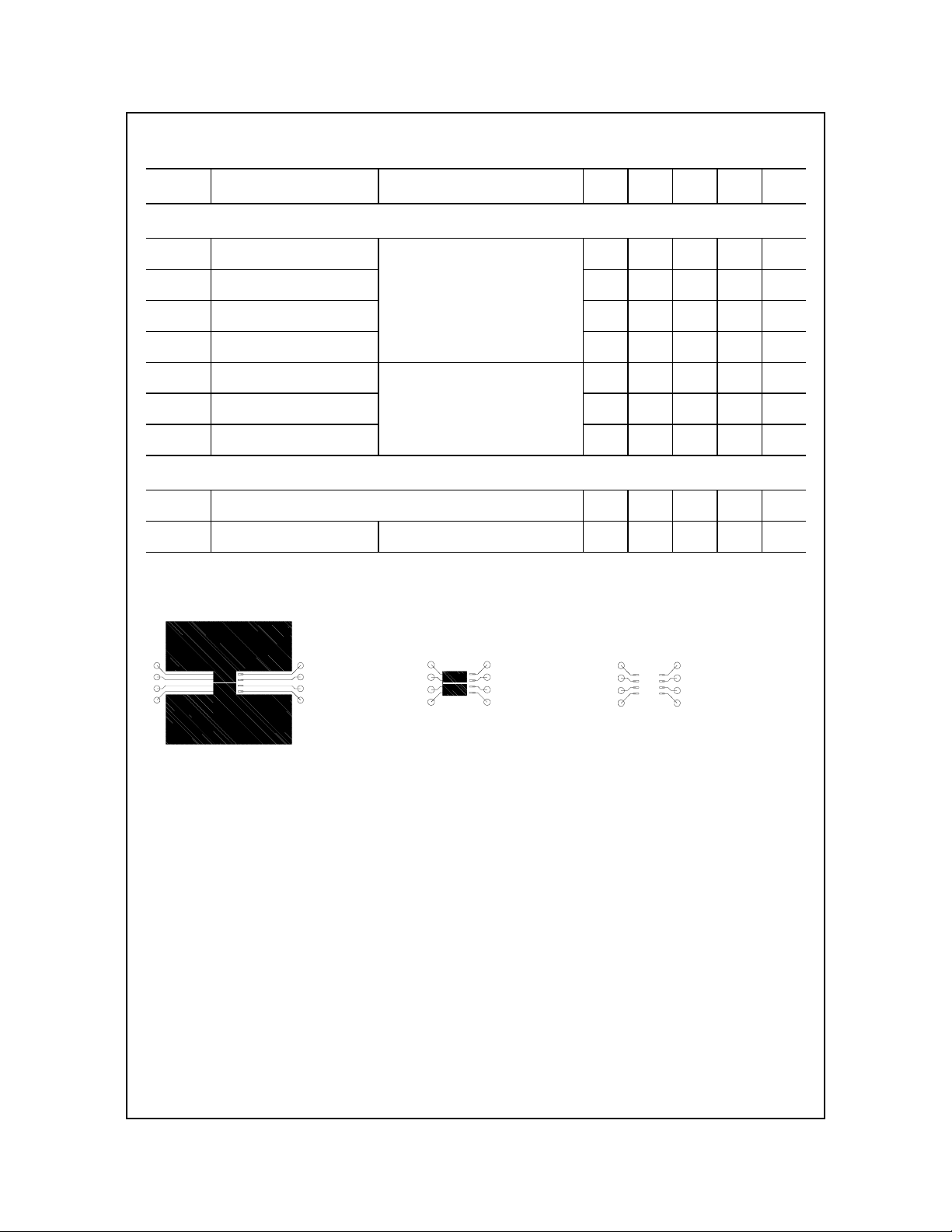
a) 78° C/W when
mounted on a 0.5 in
pad of 2 oz. copper.
Scale 1 : 1 on letter size paper
2. Pulse Test: Pulse Width ≤ 300 µs, Duty Cycle ≤ 2.0%
2
b) 125° C/W when
mounted on a 0.02 in
pad of 2 oz. copper.
2
c) 135° C/W when
mounted on a 0.003 in
pad of 2 oz. copper.
2
FDS6982, Rev. C

Typical Characteristics: Q2
FDS6982
50
VGS = 10V
5.0V
40
30
20
10
0
01234
4.5V
4.0V
V
, DRAIN-SOURCE VOLTAGE (V)
DS
3.5V
3.0V
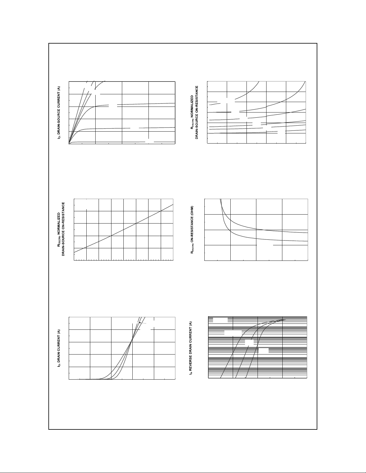
Figure 1. On-Region Characteristics.
1.6
ID = 8.6A
V
= 10V
GS
1.4
1.2
1
0.8
2
1.8
VGS = 4.0V
1.6
1.4
1.2
1
0.8
0 1020304050
4.5V
5.0V
, DRAIN CURRENT (A)
I
D
6.0V
7.0V
10V
Figure 2. On-Resistance Variation
with Drain Current and Gate V oltage.
0.04
0.03
0.02
0.01
TA = 125oC
TA = 25oC
ID = 4.5A
0.6
-50 -25 0 25 50 75 100 125 150
, JUNCTION TEMPERATURE (oC)
T
J
Figure 3. On-Resistance Variation
with Temperature.
50
VDS = 5V
40
30
20
10
0
123456
V
, GATE TO SOURCE VOLTAGE (V)
GS
TA = -55oC
25oC
125oC
Figure 5. Transfer Characteristics.
0
246810
, GATE TO SOURCE VOLTAGE (V)
V
GS
Figure 4. On-Resistance Variation
with Gate-to-Source Voltage.
100
VGS = 0V
10
1
0.1
0.01
0.001
0.0001
TA = 125oC
25oC
-55oC
0 0.4 0.8 1.2 1.6
, BODY DIODE FORWARD VOLTAGE (V)
V
SD
Figure 6. Body Diode Forward Voltage
Variation with Source Current
and Temperature.
FDS6982, Rev. C
 Loading...