

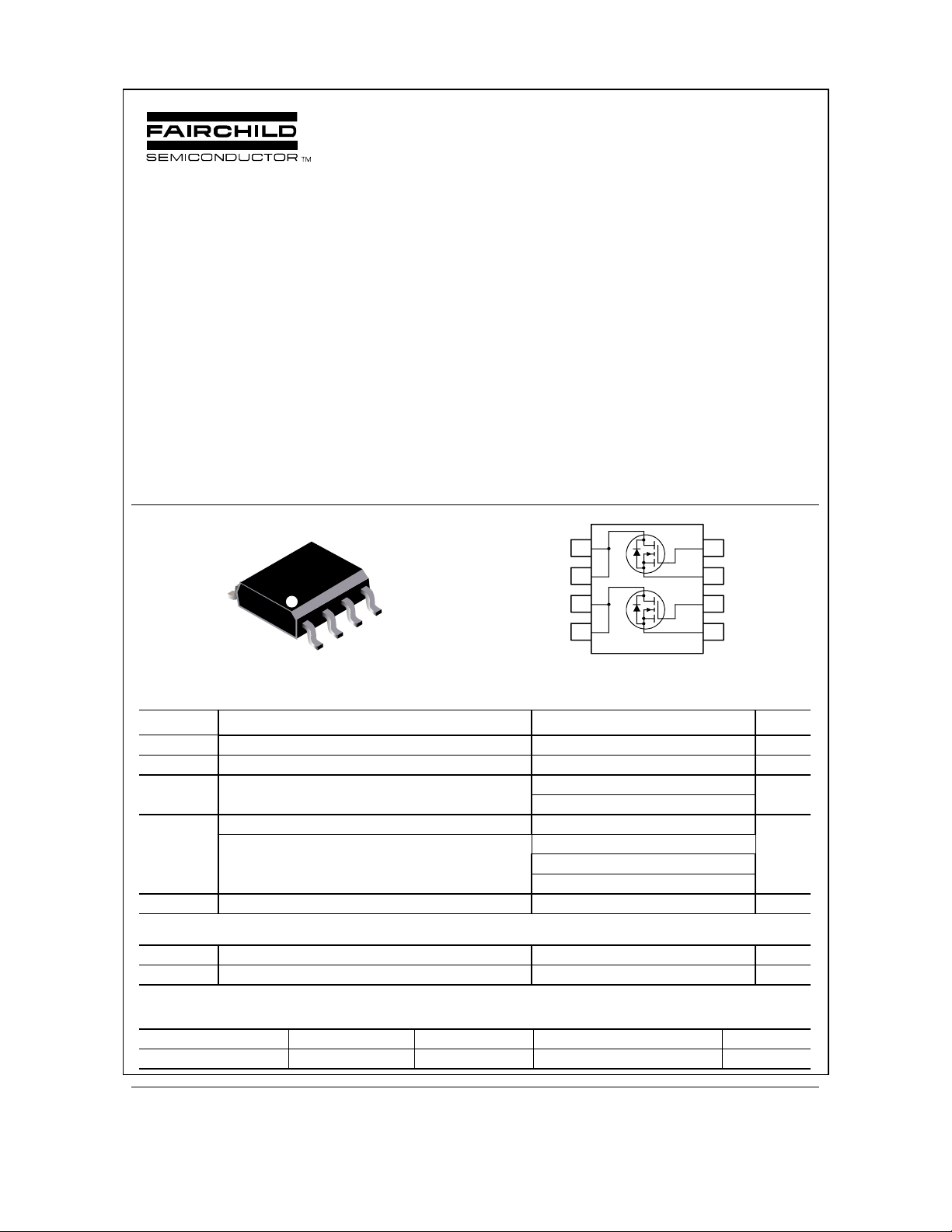
Fairchild Semiconductor FDS6912 Datasheet
January 2000
FDS6912
Dual N-Channel Logic Level PWM Optimized PowerTrench MOSFET
FDS6912
General Description
These N-Channel Logic Level MOSFETs have been
designed specifically to improve the overall effici ency of
DC/DC converters using either synchronous or
conventional switching PWM controllers.
These MOSFETs feature faster switching and lower
gate charge than other MOSFETs with comparable
RDS(ON) specifications.
The result is a MOSFET that is easy and safer to drive
Features
6 A, 30 V. R
•
R
= 0.042 Ω @ VGS = 4.5 V.
DS(ON)
Optimized for use in switching DC/DC converters
•
with PWM controllers
Very fast switching.
•
Low gate charge
•
= 0.028 Ω @ VGS = 10 V
DS(ON)
(even at very high frequencies), and DC/DC power
supply designs with higher overall efficiency.
D1
D1
D2
D2
G1
S2
S1
G2
SO-8
Absolute Maximum Ratings
TA=25oC unless otherwise noted
5
Q1
6
7
Q2
8
4
3
2
1
Symbol Parameter Ratings Units
V
DSS
V
GSS
I
D
P
D
TJ, T
stg
Drain-Source Voltage 30 V
Gate-Source Voltage
Drain Current – Continuous
(Note 1a)
20
±
6A
– Pulsed 20
Power Dissipation for Dual Operation 2
Power Dissipation for Single Operation
(Note 1a)
(Note 1b)
(Note 1c)
1.6
1
0.9
Operating and Storage Junction Temperature Range -55 to +150
V
W
C
°
Thermal Characteristics
R
JA
θ
R
JC
θ
Thermal Resistance, Junction-to-Ambient
Thermal Resistance, Junction-to-Case
(Note 1a)
(Note 1)
78
40
Package Marking and Ordering Information
Device Marking Device Reel Size Tape width Quantity
FDS6912 FDS6912 13’’ 12mm 2500 units
2000 Fairchild Semiconductor Corpor ation
C/W
°
C/W
°
FDS6912 Rev E (W)
FDS6912
Electrical Characteristics
TA = 25°C unless otherwise noted
Symbol Parameter Test Conditions Min Typ Max Units
Off Characteristics
BV
DSS
BV
∆
T
∆
I
DSS
I
GSSF
I
GSSR
On Characteristics
V
GS(th)
GS(th)
V
∆
T
∆
R
DS(on)
I
D(on)
g
FS
Drain–Source Breakdown Voltage
Breakdown Voltage Temperature
DSS
Coefficient
J
V
= 0 V, ID = 250 µA
GS
= 250 µA, Referenced to 25°C
I
D
30 V
20
Zero Gate Voltage Drain Current VDS = 24 V, VGS = 0 V
T
= 55°C
J
Gate–Body Leakage, Forward VGS = 20 V, VDS = 0 V 100 nA
Gate–Body Leakage, Reverse VGS = –20 V VDS = 0 V –100 nA
(Note 2)
Gate Threshold Voltage
Gate Threshold Voltage
Temperature Coefficient
J
Static Drain–Source
On–Resistance
V
= VGS, ID = 250 µA
DS
I
= 250 µA, Referenced to 25°C
D
VGS = 10 V, ID = 6 A
T
= 125°C
J
123 V
–5
0.024
0.034
VGS = 4.5 V, ID = 4.9 A 0.035 0.042
On–State Drain Current VGS = 10 V, VDS = 5 V 20 A
Forward Transconductance VDS = 10 V, ID = 6 A 20 S
1
10
0.028
0.048
mV/°C
A
µ
mV/°C
Ω
Dynamic Characteristics
C
iss
C
oss
C
rss
Input Capacitance 740 pF
Output Capacitance 170 pF
Reverse Transfer Capacitance
= 15 V, V
V
DS
f = 1.0 MHz
GS
= 0 V,
75 pF
Switching Characteristics
t
t
t
t
Q
Q
Q
d(on)
r
d(off)
f
g
gs
gd
Turn–On Delay Time 8 16 ns
Turn–On Rise Time 13 24 ns
Turn–Off Delay Time 18 29 ns
Turn–Off Fall Time
Total Gate Charge 7 10 nC
Gate–Source Charge 3.8 nC
Gate–Drain Charge
(Note 2)
V
= 15 V, ID = 1 A,
DD
= 10 V, R
V
GS
= 10 V, ID = 6 A,
V
DS
= 5 V
V
GS
GEN
= 6
Ω
816ns
2.5 nC
Drain–Source Diode Characteristics and Maximum Ratings
I
S
V
SD
Notes:
is the sum of the junction-to-case and case-to-ambient thermal resistance where the case thermal reference is defined as the solder mounting surface of
R
1.
JA
θ
the drain pins. R
Scale 1 : 1 on letter size paper
2.
Maximum Continuous Drain–Source Diode Forward Current 1.3 A
Drain–Source Diode Forward
VGS = 0 V, IS = 1.3 A
(Note 2)
0.75 1.2 V
Voltage
is guaranteed by design while R
JC
θ
a) 78°/W when
mounted on a 0.5in
pad of 2 oz copper
Pulse Test: Pulse Width < 300µs, Duty Cycle < 2.0%
is determined by the user's board design.
CA
θ
2
b) 125°/W when
mounted on a 0.02
in2 pad of 2 oz
copper
c) 135°/W when mounted on a
minimum mounting pad.
FDS6912 Rev E (W)
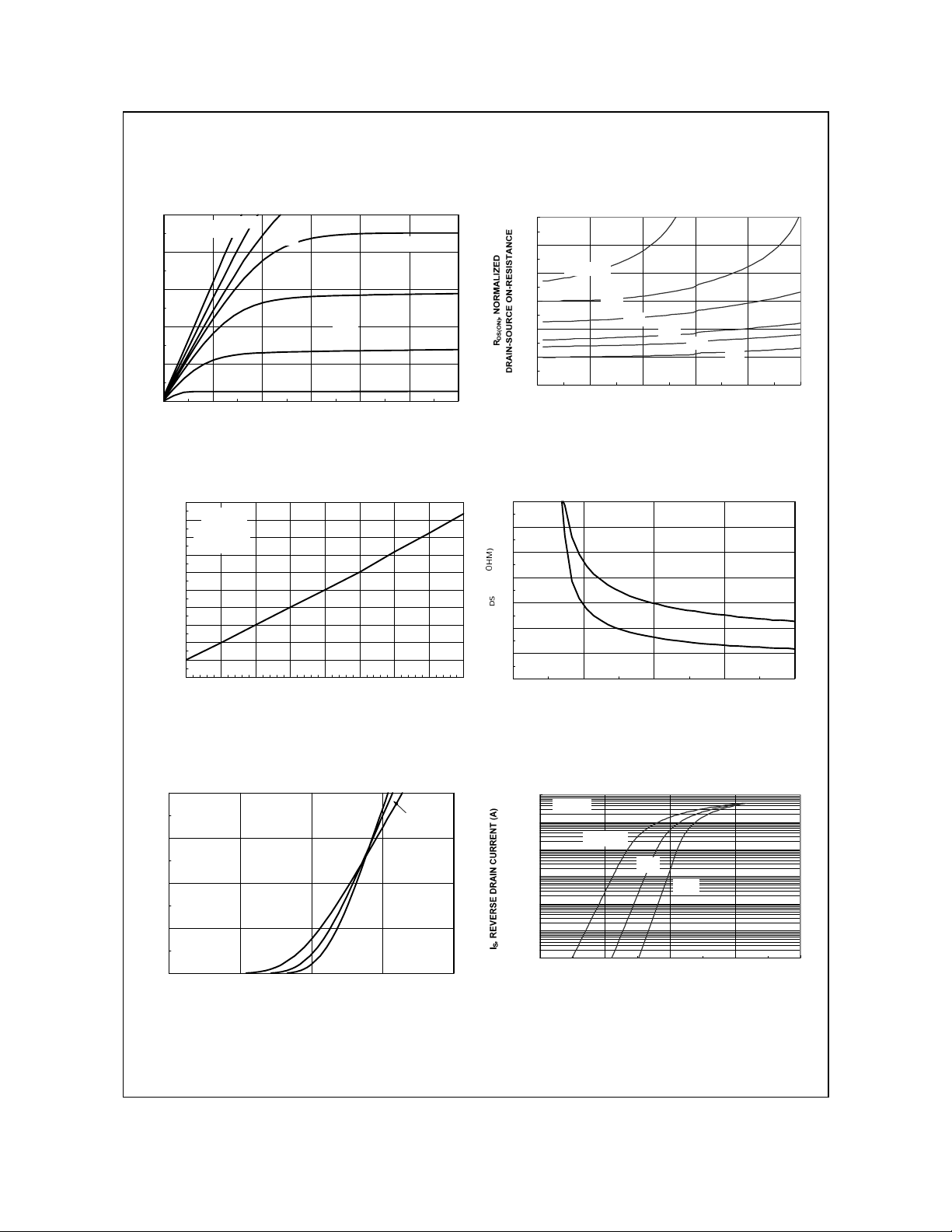
Typical Characteristics
FDS6912
30
24
18
V = 10 V
GS
6.0V
5.0V
4.5V
4.0V
12
D
I , DRAIN- S OUR CE CURREN T (A)
6
3.5V
3.0V
0
0112233
V , D RA I N-S OUR CE VOLTAGE (V)
DS
2
1.8
1.6
1.4
1.2
VGS = 4.0V
4.5V
5.0V
6.0V
7.0V
1
0.8
0 1020304050
, DRAIN CURRENT (A)
I
D
Figure 1. On-Region Characteristics. Figure 2. On-Resistance Variation with
Drain Current and Gate Voltage.
1.6
1.5
I = 6.3A
D
1.4
V =10V
GS
1.3
1.2
1.1
1.0
0.9
DS(ON)
R ,NORMALIZED
0.8
DRAIN-SOURCE ON-RESISTANCE
0.7
0.6
-50 -25 0 25 50 75 100 125 150
T , JUNCTION TEMPERATURE (°C)
J
8
7
)
6
5
4
DS(ON)
R ,(
3
DRAIN-SOURCE ON-RESISTANCE
2
1
246810
V ,GATE-SOURCE VOLTAGE (V)
GS
T = 125 C
A
o
25 C
10V
I = 3.0A
D
o
Figure 3. On-Resistance Variation
withTemperature.
20
V = 5V
DS
15
10
D
5
I , DRAIN CURRENT (A)
0
12345
V , GATE TO SOURCE VOLTAGE (V)
GS
T = -55°C
J
25°C
125°C
Figure 4. On-Resistance Variation with
Gate-to-Source Voltage.
100
VGS = 0V
10
1
0.1
0.01
0.001
0.0001
0 0.4 0.8 1.2 1.6
TA = 125oC
25oC
-55oC
, BODY DIODE FORWARD VOLTAGE (V)
V
SD
Figure 5. Transfer Characteristics. Figure 6. Body Diode Forward Voltage Variation
with Source Current and Temperature.
FDS6912 Rev E (W)
 Loading...