

Fairchild Semiconductor FDS6890A Datasheet
FDS6890A
Dual N-Channel 2.5V Specified PowerTrenchTM MOSFET
FDS6890A
November 1999
General Description
These N-Channel 2.5V specified MOSFETs are
produced using Fairchild Semiconductor's advanced
PowerTrench process that has been especially tailored
to minimize the on-state resistance and yet maintain
low gate charge for superior switching performance.
Features
•
7.5 A, 20 V. R
R
DS(ON)
DS(ON
= 0.018 Ω @ V
= 0.022 Ω @ V
)
• Low gate charge (23nC typical).
= 4.5 V
GS
= 2.5 V.
GS
• Fast switching speed.
Applications
• DC/DC converter
• Motor drives
• High performance trench technology for extremely
low R
DS(ON
.
)
• High power and current handling capability.
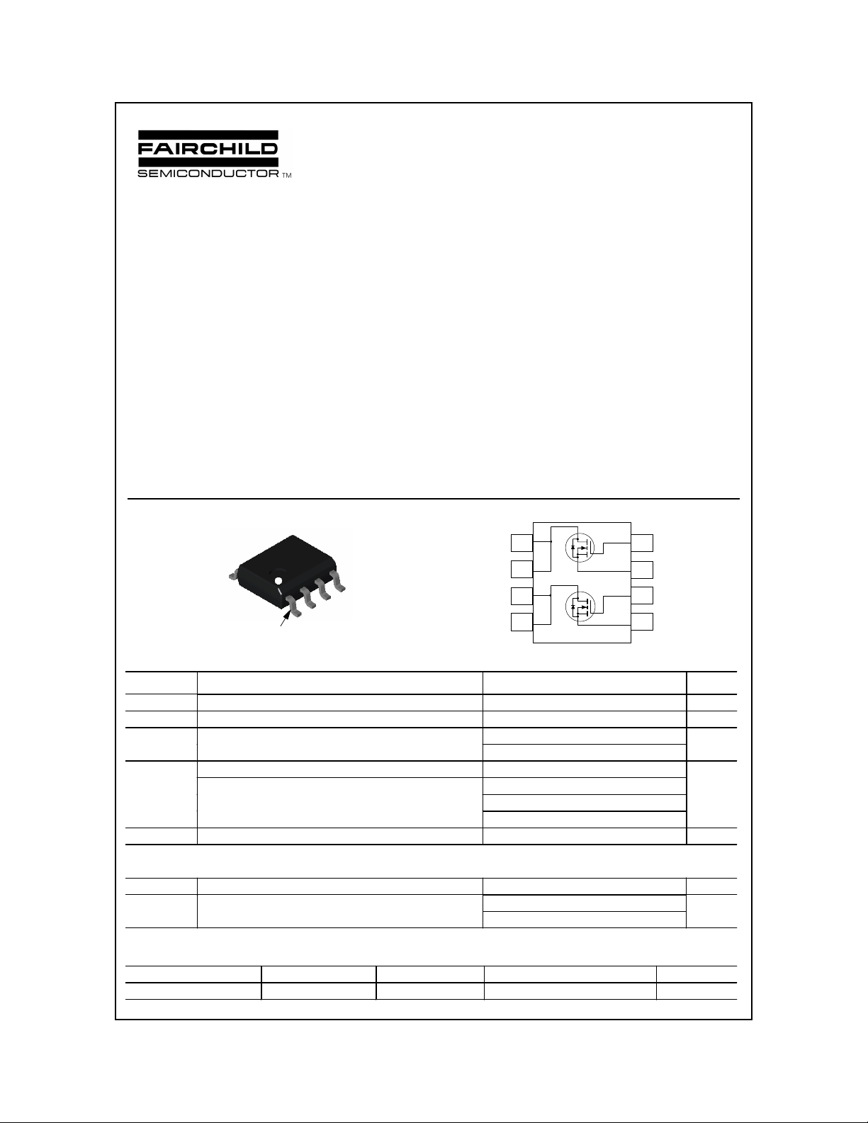
D2
D2
D1
D1
S2
G1
1
pin
SO-8
S1
Absolute Maximum Ratings
G2
T
=25oC unless otherwise noted
A
5
6
7
8
4
3
2
1
Symbol Parameter Ratings Units
V
DSS
V
GSS
I
D
P
D
TJ, T
stg
Drain-Source Voltage 20 V
Gate-Source Voltage
Drain Current - Continuous
- Pulsed 20
Power Dissipation for Dual Operation 2.0
Power Dissipation for Single Operation
Operating and Storage Junction Temperature Range -55 to +150
(Note 1a)
(Note 1a)
(Note 1b)
(Note 1c)
±
8
7.5 A
1.6
1.0
0.9
V
W
°
C
Thermal Characteristics
R
JA
θ
R
JC
θ
Thermal Resistance, Junction-to-Ambient
Therm al R es istan c e, J un ctio n-to-C as e
(Note 1a)
(Note 1)
78
40
90
Package Marking and Ordering Information
Device Marking Device Reel Size Tape Width Quantity
FDS6890A FDS6890A 13 12mm 2500 units
1999 Fairchild Semiconductor Corporation
°
C/W
°
C/W
FDS6890A Rev. C
FDS6890A
Electrical Characteristics T
Symbol
Off Characteristics
BV
∆
∆
I
DSS
I
GSSF
DSS
BV
T
Drain-Source Breakdown Voltage
Breakdown Voltage Temperature
DSS
Coefficient
J
Zero Gate Voltage Drain Current VDS = 16 V, VGS = 0 V 1
Gate-Body Leakage Current,
Parameter
= 25 C unless otherwise noted
A
Test Conditions
V
= 0 V, ID = 250 µA
GS
= 250 µA, Referenced to 25°C
I
D
Min
Typ Max Units
20 V
14
VGS = 8 V, VDS = 0 V 100 nA
mV/°C
µ
A
Forward
I
Gate-Body Leakage Current,
GSSR
On Characteristics
V
GS(th)
∆
GS(th)
V
∆
T
R
DS(on)
Reverse
(Note 2)
Gate Threshold Voltage
Gate Threshold Voltage
Temperature Coefficient
J
Static Drain-Source
On-Resistance
I
On-State Drain Current VGS = 10 V, VDS = 5 V 20 A
D(on)
VGS = -8 V, VDS = 0 V -100 nA
V
= VGS, ID = 250 µA
DS
= 250 µA, Referenced to 25°C
I
D
0.5 0.8 1.5 V
-3.5
mV/°C
VGS = 4.5 V, ID =7.5 A
= 4.5 V, ID =7.5 A, TJ =125°C
V
GS
= 2.5 V, ID =6.5 A
V
GS
0.013
0.021
0.016
0.018
0.034
0.022
Ω
gFS Forward Transconductance VDS = 5 V, ID = 7.5 A 35 S
Dynamic Characteristics
C
Input Capacitance 2130 pF
iss
C
Output Capacitance 545 pF
oss
C
Revers e Transfer Capacitance
rss
Switching Characteristics
t
Turn-On Delay Time 13 24 ns
d(on)
tr Turn-On Rise Time 26 42 ns
t
Turn-Off Del ay Ti me 65 90 ns
d(off)
tf Turn-Off Fall Time
Qg Total Gate Charge 23 32 nC
Qgs Gate-Source Charge 3.2 nC
Qgd Gate-Drain Charge
Drain-Source Diode Characteristics and Maximum Ratings
= 10 V, VGS = 0 V,
V
DS
f = 1.0 MHz
270 pF
(Note 2)
V
= 10 V, ID = 1 A,
DD
= 4.5 V, R
V
GS
GEN
= 6 Ω
23 37 ns
= 10 V, ID = 7.5 A,
V
DS
= 4.5 V,
V
GS
4.4 nC
IS Maximum Continuous Drain-Source Diode Forward Current 1.3 A
VSD Drain-Sourc e Di ode Forward
VGS = 0 V, IS = 1.3 A
(Note 2)
0.65 1.2 V
Voltage
Notes:
1. R
surface of the drain pins. R
is the sum of the junction-to-case and case-to-ambient thermal resistance where the case thermal reference is defined as the solder mounting
θJA
is guaranteed by design while R
θJC
is determined by the user's board design.
θCA
Scale 1 : 1 on letter size paper
a) 78° C/W when
mounted on a 0.5 in
pad of 2 oz. copper.
2
b) 125° C/W when
mounted on a 0.02 in
pad of 2 oz. copper.
2
c) 135° C/W when
mounted on a minimum pad.
FDS6890A Rev. C
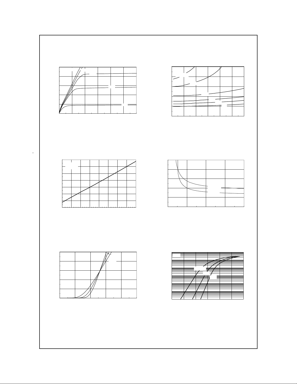
T ypical Characteristics (continued)
FDS6890A
30
VGS=4.5V
2.5V
24
18
12
6
, DRAIN-SOURCE CURRENT (A)
D
I
0
00.511.522.53
2.0V
, DRAIN-SOURCE VOLTAGE (V)
V
DS
1.8
VGS =1.8V
1.6
1.4
, NORMALIZED
1.2
DS(ON)
R
1
2.0V
2.5V
3.0V
3.5V
DRAIN-SOURCE ON-RESISTANCE
0.8
0 5 10 15 20 25 30
I
, DRAIN CURRENT (A)
D
4.5
Figure 1. On-Region Characteristics. Figure 2. On-Resistance V ariation with
Drain Current and Gate V oltage.
1.8
ID = 7.5A
1.6
V
= 4.5V
GS
1.4
1.2
1
, NORMALIZED
DS(ON)
0.8
R
0.6
DRAIN-SOURCE ON-RES ISTANCE
0.4
-50-25 0 255075100125150
, JUNCTION TEMPERATURE (oC)
T
J
0.05
0.04
0.03
0.02
, ON-RESISTANCE (OHM)
0.01
DS(ON)
R
0
12345
, GATE TO SOURCE VOLT AGE (V)
V
GS
TA = 125oC
TA = 25oC
ID =3.8A
Figure 3. On-Resistance Variation
withT emperature.
30
VDS = 5V
24
18
12
, DRAIN CURRENT (A)
D
I
6
0
0.5 1 1.5 2 2.5 3
V
TA = -55oC
125oC
, GATE TO SOURCE VOLTAGE (V)
GS
25oC
Figure 5. Transfer Characteristics.
Figure 4. On-Resistance Variation with
Gate-to-Source V oltage.
100
VGS=0
10
1
0.1
0.01
0.001
, REVERSE DRAIN CURRENT (A)
S
I
0.0001
0 0.2 0.4 0.6 0.8 1 1.2
TJ=125oC
25oC
-55oC
V
, BODY DIODE VOLTAGE (V)
SD
Figure 6. Body Diode Forward V oltage
Variation with Source Current
and Temperature.
FDS6890A Rev. C
 Loading...