

Fairchild Semiconductor FDS6814 Datasheet
ADVANCE INFORMATION
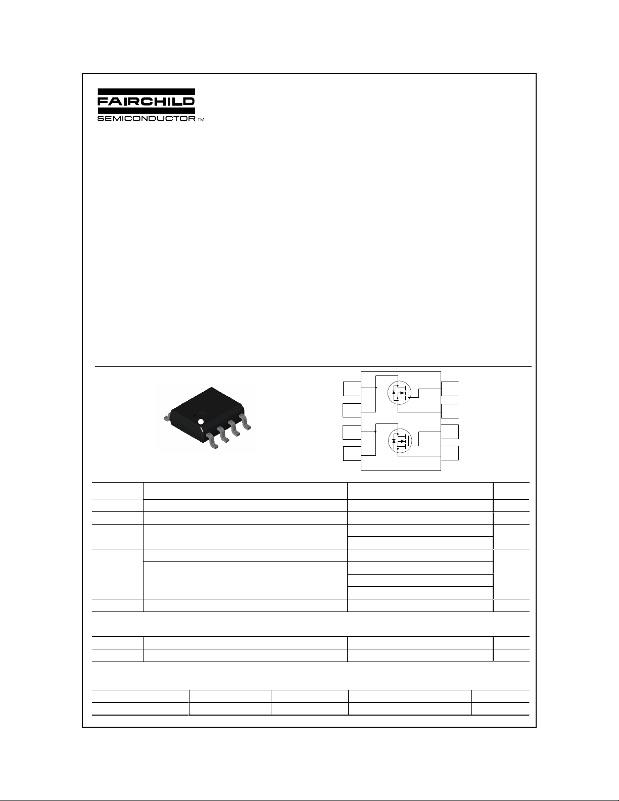
FDS6814
Dual N-Channel 2.5V Specified PowerTrenchTM MOSFET
FDS6814
July 1999
General Description
These N-Channel 2.5V specified MOSFETs are produced
using a rugged gate version of Fairchild's advanced
PowerTrenchTM process. It has been optimized for
power management applications which require a wide
range of gate drive voltage.
Features
8 A, 20 V. R
= 0.020 Ω @ V
DS(ON)
= 0.030 Ω @ V
R
DS(ON)
Rugged gate rating ( ±12V).
= 4.5 V
GS
= 2.5 V
GS
Low gate charge.
Applications
Low voltage DC/DC Converters
Load switch
Battery protection
Power management
D2
D2
Fast switching speed.
High performance trench technology for extremely
low R
DS(ON)
.
High power and current handling capability.
5
4
D1
D1
G2
S2
SO-8
G1
S1
Absolute Maximum Ratings
=25oC unless otherwise noted
T
A
6
7
8
3
2
1
Symbol Parameter Ratings Units
V
DSS
V
GSS
I
D
P
D
TJ, T
stg
Drain-Source Voltage 20 V
Gate-Source Voltage
Drain Current - Continuous
- Pulsed 50
Power Dissipation for Dual Operation 2.0
Power Dissipation for Single Operation
(Note 1b)
(Note 1c)
Operating and Storage Junction Temperature Range -55 to +150
(Note 1a)
(Note 1a)
±12
8A
1.6
1.0
0.9
V
W
°
C
Thermal Characteristics
R
JA
θ
R
JC
θ
Thermal Resistance, Junc tion-to-Ambient (Note 1a) 78
Thermal Resistance, Junc tion-to-Cas e (Note 1) 40
Package Marking and Ordering Information
Device Marking Device Reel Size Tape width Quantity
FDS6814 FDS6814 13’’ 12mm 2500 units
1999 Fairchild Semiconductor Corporation
°
C/W
°
C/W
FDS6814 Rev. A
FDS6814
Electrical Characteristics T
=25oC unless otherwise noted
A
Symbol Parameter Test Conditions Min Typ Max Units
OFF CHARACTERISTICS
BV
I
DSS
I
GSSF
I
GSSR
DSS
Drain-Source Breakdown Voltage
= 0 V, ID = 250 µA
V
GS
Zero Gate Voltage Drain Current VDS = 16 V, VGS = 0 V 1
Gate-Body Leakage, Forward VGS = 12 V, VDS = 0 V 100 nA
Gate-Body Leakage, Reverse VGS = -12 V, VDS = 0 V -100 nA
20 V
µA
ON CHARACTERISTICS (Note 2)
V
GS(TH)
R
DS(ON)
I
D(ON)
Gate Threshold Voltage
Static Drain-Source
On-Resistance
= VGS, ID = 250 µA
V
DS
VGS = 4.5 V, ID = 8 A
V
= 2.5 V, ID = 6.5 A
GS
On-State Drain Current VGS = 4.5 V, VDS = 5.0 V 25 A
0.6 1.5 V
0.02
0.03
Ω
DRAIN-SOURCE DIODE CHARACTERISTICS AND MAXIMUM RATINGS
I
S
V
SD
Notes:
1. R
R
θJA
θJC
Maximum Continuous Drain-Source Diode Forward Current 1.3 A
Drain-Source Diode Forward
VGS = 0 V, IS = 1.3 A (Note 2) 1.2 V
Voltage
is the sum of the junction-to-case and case-to-ambient thermal resistance where the case thermal reference is defined as the solder mounting surface of the drain pins.
is guaranteed by design while R
is determined by the user's board design. Thermal rating based on independent single device operation.
θCA
a) 78° C/W when
mounted on a 0.5 in
pad of 2 oz. copper.
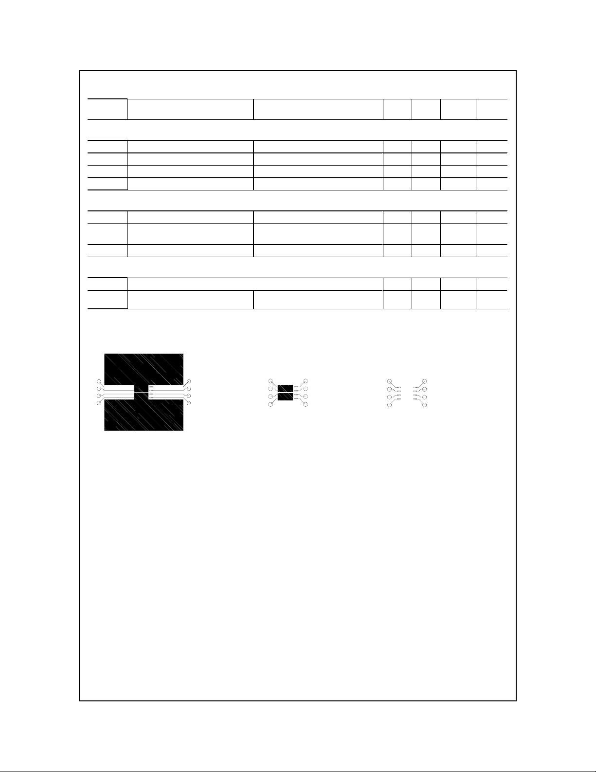
Scale 1 : 1 on letter size paper
2. Pulse Test: Pulse Width ≤ 300 µs, Duty Cycle ≤ 2.0%
2
b) 125° C/W when
mounted on a 0.02 in
pad of 2 oz. copper.
2
c) 135° C/W when
mounted on a minimum pad.
FDS6814 Rev. A
 Loading...