

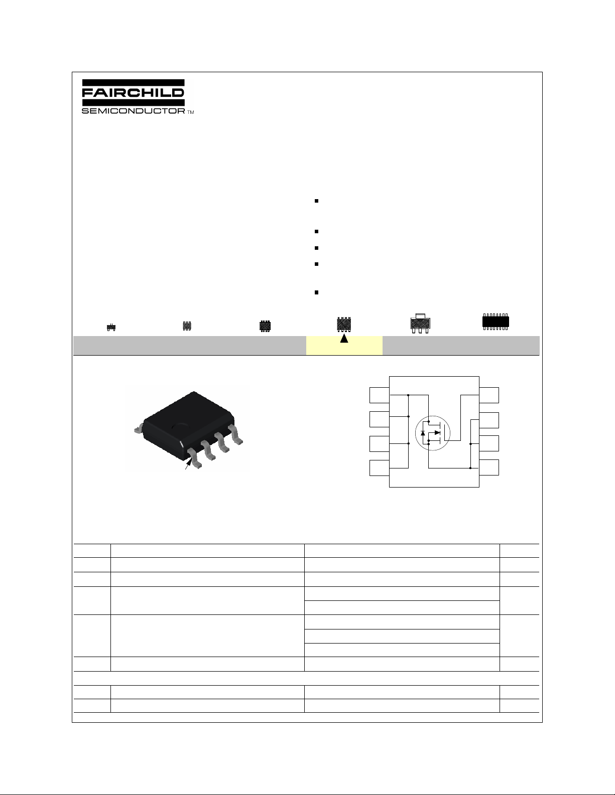
Fairchild Semiconductor FDS6690A Datasheet
April 1999
FDS6690A
Single N-Channel, Logic Level, PowerTrenchTM MOSFET
General Description Features
This N-Channel Logic Level MOSFET is
produced using Fairchild Semiconductor's
advanced PowerTrench process that has been
especially tailored to minimize the on-state
resistance and yet maintain superior switching
performance.
These devices are well suited for low voltage and
battery powered applications where low in-line
power loss and fast switching are required.
11 A, 30 V. R
Fast switching speed.
Low gate charge.
High performance trench technology for
extremely low R
High power and current handling capability.
= 0.0125 Ω @ VGS = 10 V,
DS(ON)
R
= 0.017 Ω @ VGS = 4.5 V.
DS(ON)
.
DS(ON)
SOT-23
SuperSOTTM-8
D
D
D
D
FDS
6690A
SO-8 SOT-223SuperSOTTM-6
5
6
7
SOIC-16
4
3
2
G
SO-8
1
S
pin
S
8
1
S
Absolute Maximum Ratings T
Symbol Parameter Ratings Units
V
DSS
V
GSS
I
D
P
D
TJ,T
THERMAL CHARACTERISTICS
R
JA
θ
R
JC
θ
Drain-Source Voltage 30 V
Gate-Source Voltage ±20 V
Drain Current - Continuous (Note 1a) 11 A
- Pulsed 50
Power Dissipation for Single Operation (Note 1a) 2.5 W
(Note 1b) 1.2
(Note 1c) 1
Operating and Storage Temperature Range -55 to 150 °C
STG
Thermal Resistance, Junction-to-Ambient (Note 1a) 50 °C/W
Thermal Resistance, Junction-to-Case (Note 1) 25 °C/W
= 25oC unless other wise noted
A
© 1998 Fairchild Semiconductor Corporation
FDS6690A Rev.C1
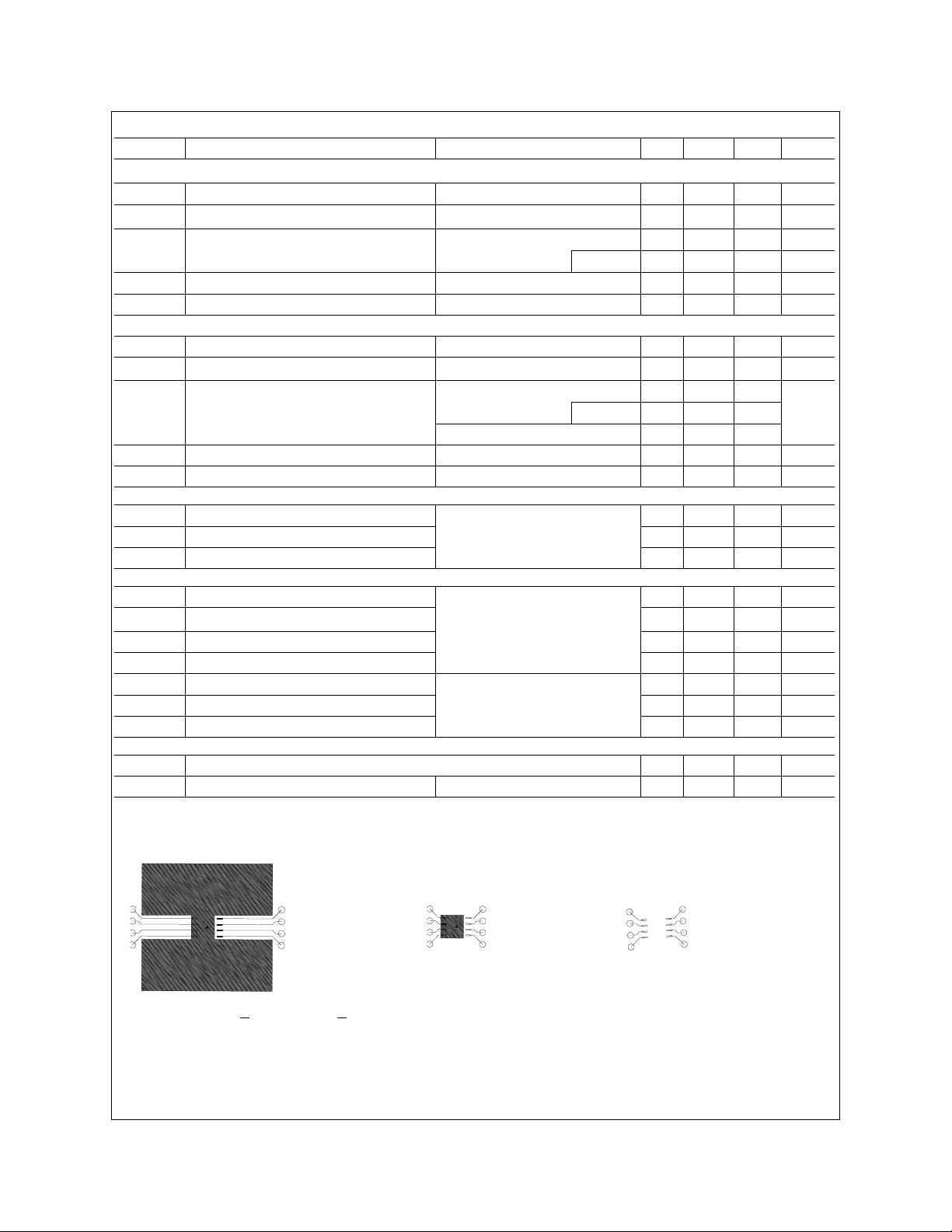
Electrical Characteristics (T
= 25 OC unless otherwise noted )
A
Symbol Parameter Conditions Min Typ Max Units
OFF CHARACTERISTICS
BV
∆BV
I
DSS
DSS
DSS
Drain-Source Breakdown Voltage VGS = 0 V, I D = 250 µA 30 V
Breakdown Voltage Temp. Coefficient ID = 250 µA, Referenced to 25 oC 20 mV / oC
/∆T
J
Zero Gate Voltage Drain Current VDS = 24 V, V
= 0 V 1 µA
GS
TJ = 55°C 10 µA
I
GSSF
I
GSSR
Gate - Body Leakage, Forward VGS = 20 V, VDS = 0 V 100 nA
Gate - Body Leakage, Reverse VGS = -20 V, VDS= 0 V -100 nA
ON CHARACTERISTICS (Note 2)
V
∆V
R
GS(th)
GS(th)
DS(ON)
Gate Threshold Voltage VDS = VGS, ID = 250 µA 1 1.5 3 V
Gate Threshold Voltage Temp. Coefficient ID = 250 µA, Referenced to 25 oC -4 mV /oC
/∆T
J
Static Drain-Source On-Resistance VGS = 10 V, I D = 11 A 0.01 0.0125
TJ =125°C 0.015 0.022
VGS = 4.5 V, I D = 10 A 0.013 0.017
I
D(ON)
g
FS
On-State Drain Current VGS = 10 V, VDS = 5 V 50 A
Forward Transconductance VDS = 15 V, I D= 11 A 45 S
DYNAMIC CHARACTERISTICS
C
iss
C
oss
C
rss
Input Capacitance VDS = 15 V, VGS = 0 V,
Output Capacitance 350 pF
f = 1.0 MHz
1600 pF
Reverse Transfer Capacitance 140 pF
SWITCHING CHARACTERISTICS (Note 2)
t
t
t
t
Q
Q
Q
D(on)
r
D(off)
f
g
gs
gd
Turn - On Delay Time VDS= 15 V, I D= 1 A 10 18 ns
Turn - On Rise Time
VGS = 10 V , R
GEN
= 6 Ω
12 22 ns
Turn - Off Delay Time 35 56 ns
Turn - Off Fall Time 10 18 ns
Total Gate Charge VDS = 15 V, I D = 11A, 17 23 nC
Gate-Source Charge VGS= 5 V 5 nC
Gate-Drain Charge 6 nC
DRAIN-SOURCE DIODE CHARACTERISTICS AND MAXIMUM RATINGS
I
S
V
SD
Notes:
1. R
JA
θ
guaranteed by design while R
Maximum Continuous Drain-Source Diode Forward Current 2.1 A
Drain-Source Diode Forward Voltage VGS = 0 V, IS = 2.1 A
is the sum of the junction-to-case and case-to-ambient thermal resistance where the case thermal reference is defined as the solder mounting surface of the drain pins. R
is determined by the user's board design.
CA
θ
(Note 2) 0.73 1.2 V
Ω
is
JC
θ
a. 50OC/W on a 1 in2 pad
of 2oz copper.
Scale 1 : 1 on letter size paper
2. Pulse Test: Pulse Width < 300µs, Duty Cycle < 2.0%.
b. 105OC/W on a 0.04 in
pad of 2oz copper.
2
c. 125OC/W on a 0.006 in2 pad
of 2oz copper.
FDS6690A Rev.C1
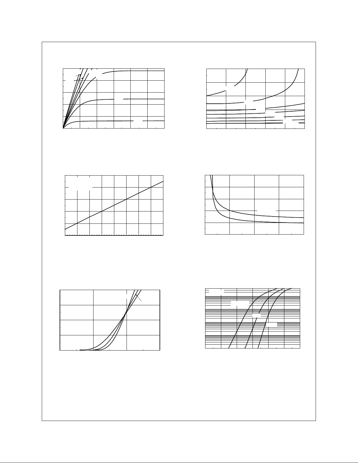
Typical Electrical Characteristics
50
V =10V
GS
6.0V
40
4.5V
30
4.0V
3.5V
3.0V
20
10
D
I , DRAIN-SOURCE CURRENT (A)
0
0 0.5 1 1.5 2 2.5 3
V , DRAIN-SOURCE VOLTAGE (V)
DS
2.5V
Figure 1. On-Region Characteristics.
1.6
I = 11A
D
V = 10V
GS
1.4
1.2
1
DS(ON)
0.8
R , NORMALIZED
DRAIN-SOURCE ON-RESISTANCE
0.6
-50 -25 0 25 50 75 100 125 150
T , JUNCTION TEMPERATURE (°C)
J
3
2.5
2
1.5
DS(ON)
R , NORMALIZED
DRAIN-SOURCE ON-RESISTANCE
1
0 10 20 30 40 50
Figure 2. On-Resistance Variation with
Drain Current and Gate Voltage.
0.05
0.04
0.03
0.02
0.01
DS(ON)
R , ON-RESISTANCE (OHM)
0
2 4 6 8 10
V = 3.0V
GS
3.5 V
4.0 V
I , DRAIN CURRENT (A)
D
T = 125°C
A
V , GATE TO SOURCE VOLTAGE (V)
GS
4.5 V
T = 25°C
A
5.5 V
7.0 V
10V
I = 5.5A
D
Figure 3. On-Resistance Variation with
Temperature.
40
V =5.0V
DS
30
T = -55°C
J
25°C
125°C
Figure 4. On Resistance Variation with
Gate-to-Source Voltage.
40
V = 0V
GS
10
T = 125°C
1
J
25°C
20
10
D
I , DRAIN CURRENT (A)
0
1 2 3 4
V , GATE TO SOURCE VOLTAGE (V)
GS
0.1
0.01
S
I , REVERSE DRAIN CURRENT (A)
0.001
0 0.2 0.4 0.6 0.8 1 1.2
V , BODY DIODE FORWARD VOLTAGE (V)
SD
-55°C
Figure 5. Transfer Characteristics. Figure 6. Body Diode Forward Voltage
Variation with Source Current
and Temperature.
FDS6690A Rev.C1
 Loading...