

Fairchild Semiconductor FDS6679Z Datasheet
FDS6679Z
FDS6679Z
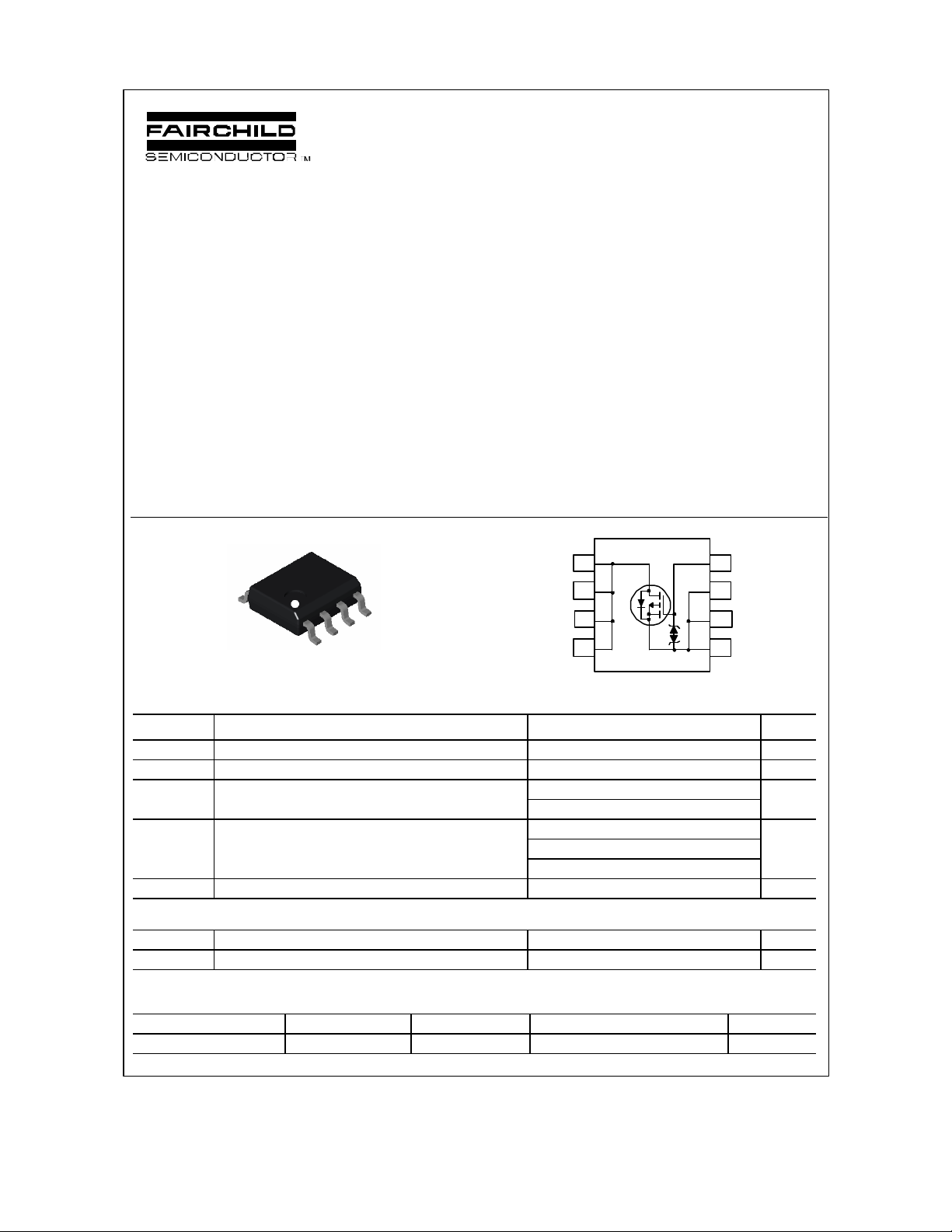
30 Volt P-Channel PowerTrench MOSFET
October 2001
General Description
This P-Channel MOSFET has been designed
specifically to improve the overall efficiency of DC/DC
converters using either synchronous or conventional
switching PWM controllers, and battery chargers.
These MOSFETs feature faster switching and lower
gate charge than other MOSFETs with comparable
R
specifications.
DS(ON)
The result is a MOSFET that is easy and safer to drive
(even at very high frequencies), and DC/DC power
supply designs with higher overall efficiency.
Features
• –13 A, –30 V. R
R
• Extended V
• ESD protection diode (note 3)
• High performance trench technology for extremely
low R
• High power and current handling capability
DS(ON)
GSS
= 9 mΩ @ VGS = –10 V
DS(ON)
= 13 mΩ @ VGS = – 4.5 V
DS(ON)
range (–25V) for battery applications
D
D
D
D
G
S
S
SO-8
S
Absolute Maximum Ratings T
o
=25
C unless otherwise noted
A
45
36
27
18
Symbol Parameter Ratings Units
V
Drain-Source Voltage –30 V
DSS
V
Gate-Source Voltage –25/+20 V
GSS
ID Drain Current – Continuous (Note 1a) –13 A
– Pulsed –50
PD
TJ, T
STG
Power Dissipation for Single Operation (Note 1a) 2.5
(Note 1b)
(Note 1c)
Operating and Storage Junction Temperature Range –55 to +175
1.2
1.0
W
°C
Thermal Characteristics
R
θJA
R
θJC
Thermal Resistance, Junction-to-Ambient (Note 1a) 50
Thermal Resistance, Junction-to-Case (Note 1) 25
°C/W
°C/W
Package Marking and Ordering Information
Device Marking Device Reel Size Tape width Quantity
FDS6679Z FDS6679Z 13’’ 12mm 2500 units
2001 Fairchild Semiconductor Corporation
FDS6679Z Rev C (W)
FDS6679Z
Electrical Characteristics T
= 25°C unless otherwise noted
A
Symbol Parameter Test Conditions Min Typ Max Units
Off Characteristics
BV
Drain–Source Breakdown Voltage VGS = 0 V, ID = –250 µA –30 V
DSS
∆BVDSS
∆TJ
I
Zero Gate Voltage Drain Current VDS = –24 V, VGS = 0 V –1 µA
DSS
I
GSSF
I
GSSR
Breakdown Voltage Temperature
Coefficient
ID = –250 µA,Referenced to 25°C –22 mV/°C
Gate–Body Leakage, Forward VGS = –25 V, VDS = 0 V –10
Gate–Body Leakage, Reverse VGS = 20 V, VDS = 0 V 10
µA
µA
On Cha racteristics (Note 2)
V
Gate Threshold Voltage VDS = VGS, ID = –250 µA –1 –1.7 –3 V
GS(th)
∆VGS(th)
∆TJ
R
DS(on)
I
D(on)
Gate Threshold Voltage
Temperature Coefficient
Static Drain–Source
On–Resistance
ID = –250 µA,Referenced to 25°C
VGS = –10 V, ID = –13 A
VGS = –4.5 V, ID = –11 A
VGS=–4.5 V, ID =–13A, TJ=125°C
4.9 mV/°C
7.2
10
10
9
13
13
m Ω
On–State Drain Current VGS = –4.5 V, VDS = –5 V –50 A
gFS Forward Transconductance VDS = –5 V, ID = –13 A 43 S
Dynamic Characteristics
C
Input Capacitance 3803 pF
iss
C
Output Capacitance 974 pF
oss
C
Reverse Transfer Capacitance
rss
VDS = –15 V, V
f = 1.0 MHz
= 0 V,
GS
490 pF
Switching Characteristics (Note 2)
t
Turn–On Delay Time 18 32 ns
d(on)
tr Turn–On Rise Time 9 18 ns
t
Turn–Off Delay Time 92 147 ns
d(off)
tf Turn–Off Fall Time
Qg Total Gate Charge 67 94 nC
Qgs Gate–Source Charge 11 nC
Qgd Gate–Drain Charge
VDD = –15 V, ID = –1 A,
VGS = –10 V, R
GEN
= 6 Ω
VDS = –15 V, ID = –13 A,
VGS = –10 V
54 86 ns
15 nC
Drain–Source Diode Characteristics and Maximum Ratings
IS Maximum Continuous Drain–Source Diode Forward Current –2.1 A
VSD
Notes:
1. R
is the sum of the junction-to-case and case-to-ambient thermal resistance where the case thermal reference is defined as the solder mounting surface of
θJA
the drain pins. R
Scale 1 : 1 on letter size paper
2. Pulse Test: Pulse Width < 300µs, Duty Cycle < 2.0%
3. The diode connected between the gate and source serves only as protection against ESD. No gate overvoltage rating is implied.
FDS6679Z Rev C(W)
Drain–Source Diode Forward
Voltage
is guaranteed by design while R
θJC
a) 50°C/W (10 sec)
62.5°C/W steady state
when mounted on a
1in2 pad of 2 oz
copper
is determined by the user's board design.
θCA
VGS = 0 V, IS = –2.1 A (Note 2) –0.7 –1.2 V
b) 105°C/W when
mounted on a .04 in2
pad of 2 oz copper
c) 125°C/W when mounted on a
minimum pad.
 Loading...