

Fairchild Semiconductor FDS6679 Datasheet
FDS6679
FDS6679
30 Volt P-Channel PowerTrench MOSFET
May 2001
General Description
This P-Channel MOSFET has been designed
specifically to improve the overall efficiency of DC/DC
converters using either synchronous or conventional
switching PWM controllers, and battery chargers.
These MOSFETs feature faster switching and lower
gate charge than other MOSFETs with comparable
R
specifications.
DS(ON)
The result is a MOSFET that is easy and safer to drive
(even at very high frequencies), and DC/DC power
supply designs with higher overall efficiency.
Features
• –13 A, –30 V. R
R
• Extended V
• High performance trench technology for extremely
low R
• High power and current handling capability
DS(ON)
GSS
= 9 mΩ @ VGS = –10 V
DS(ON)
= 13 mΩ @ VGS = – 4.5 V
DS(ON)
range (±25V) for battery applications
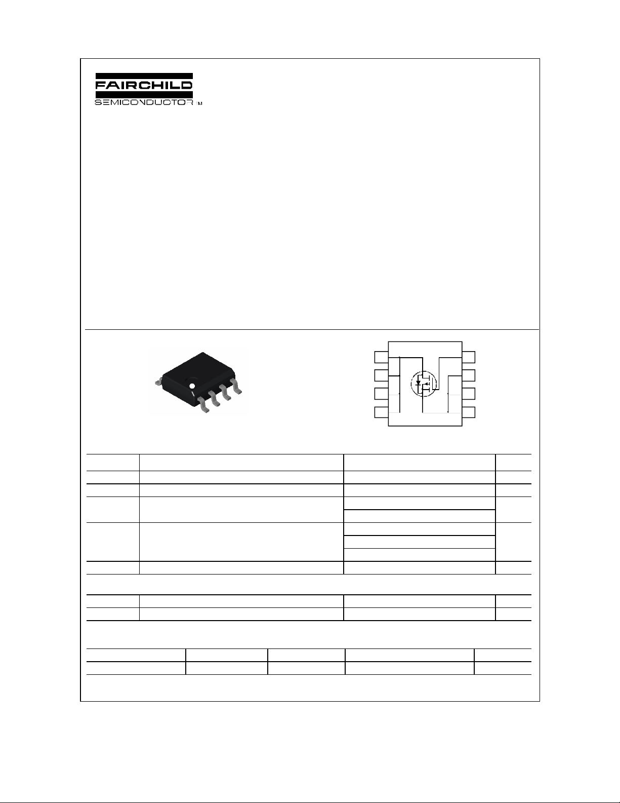
D
D
D
D
G
S
S
SO-8
S
Absolute Maximum Ratings T
o
=25
C unless otherwise noted
A
5
6
7
8
4
3
2
1
Symbol Parameter Ratings Units
V
Drain-Source Voltage –30 V
DSS
V
Gate-Source Voltage
GSS
ID Drain Current – Continuous (Note 1a) –13 A
– Pulsed –50
PD
TJ, T
STG
Power Dissipation for Single Operation (Note 1a) 2.5
(Note 1b)
(Note 1c)
Operating and Storage Junction Temperature Range –55 to +175
±25
1.2
1.0
V
W
°C
Thermal Characteristics
R
θJA
R
θJC
Thermal Resistance, Junction-to-Ambient (Note 1a) 50
Thermal Resistance, Junction-to-Case (Note 1) 25
°C/W
°C/W
Package Marking and Ordering Information
Device Marking Device Reel Size Tape width Quantity
FDS6679 FDS6679 13’’ 12mm 2500 units
2001 Fairchild Semiconductor Corporation
FDS6679 Rev C (W)
FDS6679
Electrical Characteristics T
= 25°C unless otherwise noted
A
Symbol Parameter Test Conditions Min Typ Max Units
Off Characteristics
BV
Drain–Source Breakdown Voltage VGS = 0 V, ID = –250 µA –30 V
DSS
∆BVDSS
∆TJ
I
Zero Gate Voltage Drain Current VDS = –24 V, VGS = 0 V –1 µA
DSS
I
GSSF
I
GSSR
Breakdown Voltage Temperature
Coefficient
ID = –250 µA, Referenced to 25°C –23 mV/°C
Gate–Body Leakage, Forward VGS = –25 V, VDS = 0 V 100 nA
Gate–Body Leakage, Reverse VGS = –25 V, VDS = 0 V –100 nA
On Characteristics (Note 2)
V
Gate Threshold Voltage VDS = VGS, ID = –250 µA –1 –1.6 –3 V
GS(th)
∆VGS(th)
∆TJ
R
DS(on)
I
D(on)
Gate Threshold Voltage
Temperature Coefficient
Static Drain–Source
On–Resistance
ID = –250 µA, Referenced to 25°C
VGS = –10 V, ID = –13 A
VGS = –4.5 V, ID = –11 A
VGS=–10 V, ID =–13 A, TJ=125°C
5 mV/°C
7.3
10
9.5
9
13
13
m Ω
On–State Drain Current VGS = –10 V, VDS = –5 V –50 A
gFS Forward Transconductance VDS = –5 V, ID = –13 A 44 S
Dynamic Characteristics
C
Input Capacitance 3939 pF
iss
C
Output Capacitance 972 pF
oss
C
Reverse Transfer Capacitance
rss
VDS = –15 V, V
f = 1.0 MHz
= 0 V,
GS
498 pF
Switching Characteristics (Note 2)
t
Turn–On Delay Time 19 34 ns
d(on)
tr Turn–On Rise Time 10 20 ns
t
Turn–Off Delay Time 110 176 ns
d(off)
tf Turn–Off Fall Time
Qg Total Gate Charge 71 100 nC
Qgs Gate–Source Charge 12 nC
Qgd Gate–Drain Charge
VDD = –15 V, ID = –1 A,
VGS = –10 V, R
GEN
= 6 Ω
VDS = –15 V, ID = –13 A,
VGS = –10 V
65 104 ns
15 nC
Drain–Source Diode Characteristics and Maximum Ratings
IS Maximum Continuous Drain–Source Diode Forward Current –2.1 A
VSD
Notes:
1. R
is the sum of the junction-to-case and case-to-ambient thermal resistance where the case thermal reference is defined as the solder mounting surface of
θJA
the drain pins. R
Scale 1 : 1 on letter size paper
2. Pulse Test: Pulse Width < 300µs, Duty Cy cle < 2.0%
Drain–Source Diode Forward
Voltage
is guaranteed by design while R
θJC
a) 50°C/W (10 sec)
62.5°C/W steady state
when mounted on a
1in2 pad of 2 oz
copper
is determined by the user's board design.
θCA
VGS = 0 V, IS = –2.1 A (Note 2) –0.7 –1.2 V
b) 105°C/W when
mounted on a .04 in2
pad of 2 oz copper
c) 125°C/W when mounted on a
minimum pad.
FDS6679 Rev C(W)
 Loading...