

Fairchild Semiconductor FDG6332C Datasheet
FDG6332C
FDG6332C
20V N & P-Channel PowerTrench MOSFETs
September 2003
General Description
The N & P-Channel MOSFETs are produced using
Fairchild Semiconductor’s advanced PowerTrench
process that has been especially tailored to minimize
on-state resistance and yet maintain superior
switching performance.
These devices have been designed to offer
exceptional power dissipation in a very small footprint
for applications where the bigger more expensive
TSSOP-8 and SSOP-6 packages are impractical.
Applications
• DC/DC converter
• Load switch
• LCD display inverter
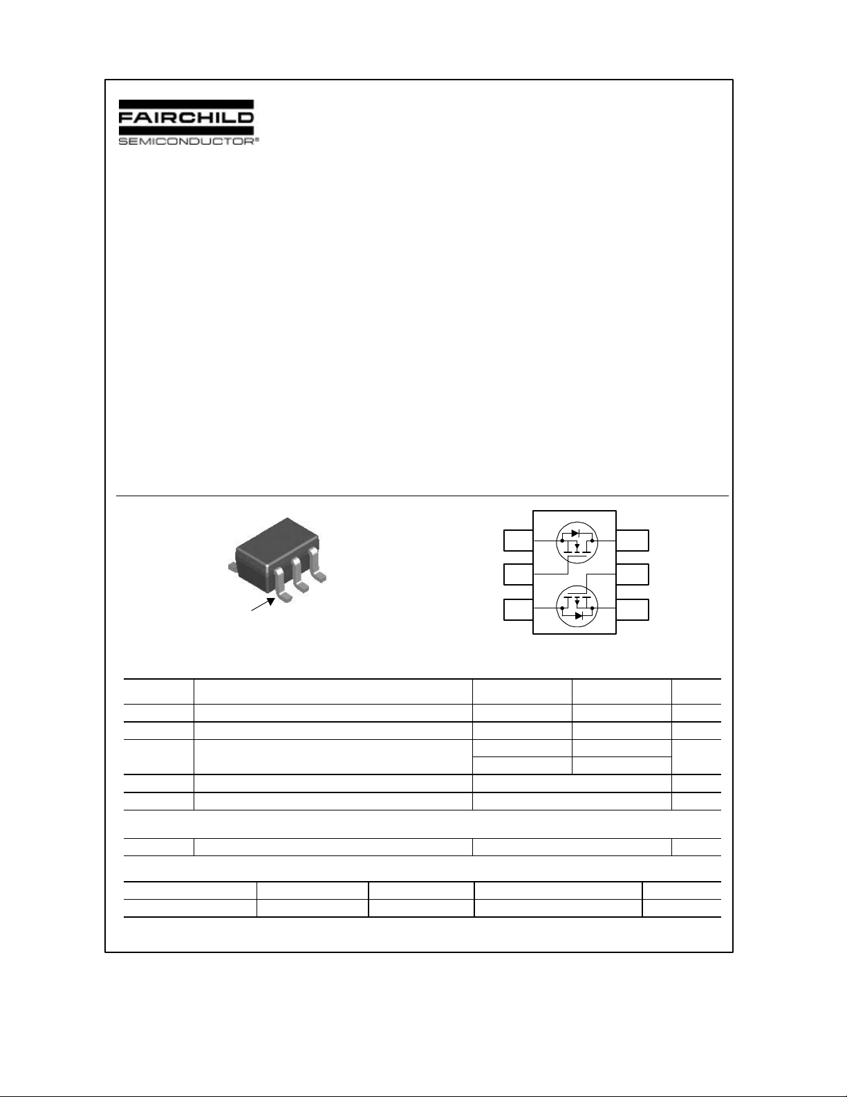
S
G
D
D
Pin 1
G
S
SC70-6
Features
• Q1 0.7 A, 20V. R
• Q2 –0.6 A, –20V. R
• Low gate charge
• High performance trench technology for extremely
low R
DS(ON)
• SC70-6 package: small footprint (51% smaller than
SSOT-6); low profile (1mm thick)
1
2
= 300 mΩ @ VGS = 4.5 V
DS(ON)
R
= 400 mΩ @ VGS = 2.5 V
DS(ON)
= 420 mΩ @ VGS = –4.5 V
DS(ON)
R
= 630 mΩ @ VGS = –2.5 V
DS(ON)
6
5
43
Complementary
Absolute Maximum Ratings T
=25oC unless otherwise noted
A
Symbol Parameter Q1 Q2 Units
V
DSS
V
GSS
I
D
P
D
TJ, T
STG
Drain-Source Voltage 20 –20 V
Gate-Source Voltage
Drain Current – Continuous (Note 1) 0.7 –0.6 A
– Pulsed 2.1 –2
Power Dissipation for Single Operation (Note 1) 0.3 W
Operating and Storage Junction Temperature Range –55 to +150 °C
±12 ±12
Thermal Characteristics
R
θJA
Thermal Resistance, Junction-to-Ambient (Note 1) 415
Package Marking and Ordering Information
Device Marking Device Reel Size Tape width Quantity
.32 FDG6332C 7’’ 8mm 3000 units
2003 Fairchild Semiconductor Corporation
FDG6332C Rev C2 (W)
V
°C/W
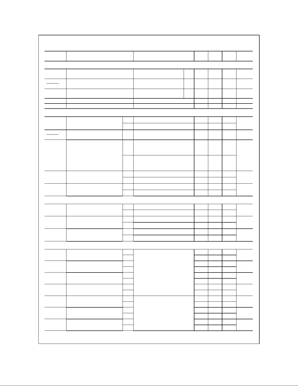
Electrical Characteristics T
GS
DS
DS
GSSF
GSSR
GSSF
GSSR
FDG6332C
= 25°C unless otherwise noted
A
Symbol Parameter Test Conditions Min Typ Max Units
Off Characteristics
BV
DSS
∆BVDSS
∆T
J
I
DSS
I
/I
I
/I
Drain–Source Breakdown Voltage
Breakdown Voltage Temperature
Coefficient
Zero Gate Voltage Drain Current
Gate–Body Leakage, Forward
Gate–Body Leakage, Reverse
= 0 V, ID = 250 µA
V
GS
V
= 0 V, ID = –250 µA
I
= 250 µA,Ref. to 25°C
D
I
= –250 µA,Ref. to 25°C
D
= 16 V, VGS = 0 V
V
V
= –16 V, VGS = 0 V Q1Q2
V
= ± 12 V, VDS = 0 V ±100
GS
V
= ± 12V , VDS = 0 V ±100
GS
Q1Q220
–20
Q1
Q2
14
–14
–1
V
mV/°C
1
µA
nA
nA
On Characteristics (Note 2)
V
GS(th)
∆VGS(th)
∆T
J
R
DS(on)
g
FS
I
D(on)
Gate Threshold Voltage
Gate Threshold Voltage
Temperature Coefficient
Static Drain–Source
On–Resistance
Forward Transconductance
On–State Drain Current
V
DS
Q1
= VGS, ID = –250 µA
V
DS
Q2
Q1
I
= 250 µA,Ref. To 25°C
D
Q2
I
= –250 µA,Ref. to 25°C
D
= 4.5 V, ID =0.7 A
V
Q1
GS
V
= 2.5 V, ID =0.6 A
GS
V
= 4.5 V, ID =0.7A,TJ=125°C
GS
V
Q2
Q1
Q2
Q1
Q2
= –4.5 V, ID = –0.6 A
GS
V
= –2.5 V, ID = –0.5 A
GS
V
=–4.5 V, ID =–0.6 A,TJ=125°C
GS
= 5 V ID = 0.7 A
V
DS
= –5 V ID = –0.6A
V
DS
= 4.5 V, VDS = 5 V
V
GS
= –4.5 V, VDS = –5 V
V
GS
0.6 1.1 1.5
-0.6 –1.2 –1.5
–2.8
3
180
300
400
293
442
247
300
420
470
630
700
400
2.8
1.8
1
–2
V
mV/°C
mΩ
S
A
= VGS, ID = 250 µA
Dynamic Characteristics
C
iss
C
oss
C
rss
Input Capacitance
Output Capacitance
Reverse Transfer Capacitance
Q1
Q2
Q1
Q2
Q1
Q2
V
DS
V
=–10 V, V
DS
=10 V, V
V
DS
=–10 V, V
V
DS
=10 V, V
V
DS
=–10 V, V
V
DS
=10 V, V
= 0 V, f=1.0MHz
GS
= 0 V, f=1.0MHz
GS
= 0 V, f=1.0MHz
GS
= 0 V, f=1.0MHz
GS
= 0 V, f=1.0MHz
GS
= 0 V, f=1.0MHz
GS
113
114
34
24
16
9
pF
pF
pF
Switching Characteristics (Note 2)
t
t
t
t
Q
Q
Q
d(on)
r
d(off)
f
Turn–On Delay Time
Turn–On Rise Time
Turn–Off Delay Time
Turn–Off Fall Time
Q1
Q2
Q1
Q2
Q1
Q2
Q1
For Q1:
V
=10 V, I D= 1 A
DS
V
= 4.5 V, R
GS
For Q2:
V
=–10 V, I D= –1 A
DS
V
= –4.5 V, R
GS
GEN
GEN
= 6 Ω
= 6 Ω
Q2
g
gs
gd
Total Gate Charge
Gate–Source Charge
Gate–Drain Charge
Q1
Q2
Q1
Q2
Q1
Q2
For Q1:
V
=10 V, I D= 0.7 A
DS
V
= 4.5 V, R
GS
For Q2:
V
=–10 V, I D= –0.6 A
DS
V
= –4.5 V, R
GS
GEN
GEN
= 6 Ω
= 6 Ω
5 10
5.5 11
7 15
14 25
9 18
6 12
1.5 3
1.7 3.4
1.1 1.5
1.4 2
0.24
0.3
0.3
0.4
ns
ns
ns
ns
nC
nC
nC
FDG6332C Rev C2 (W)
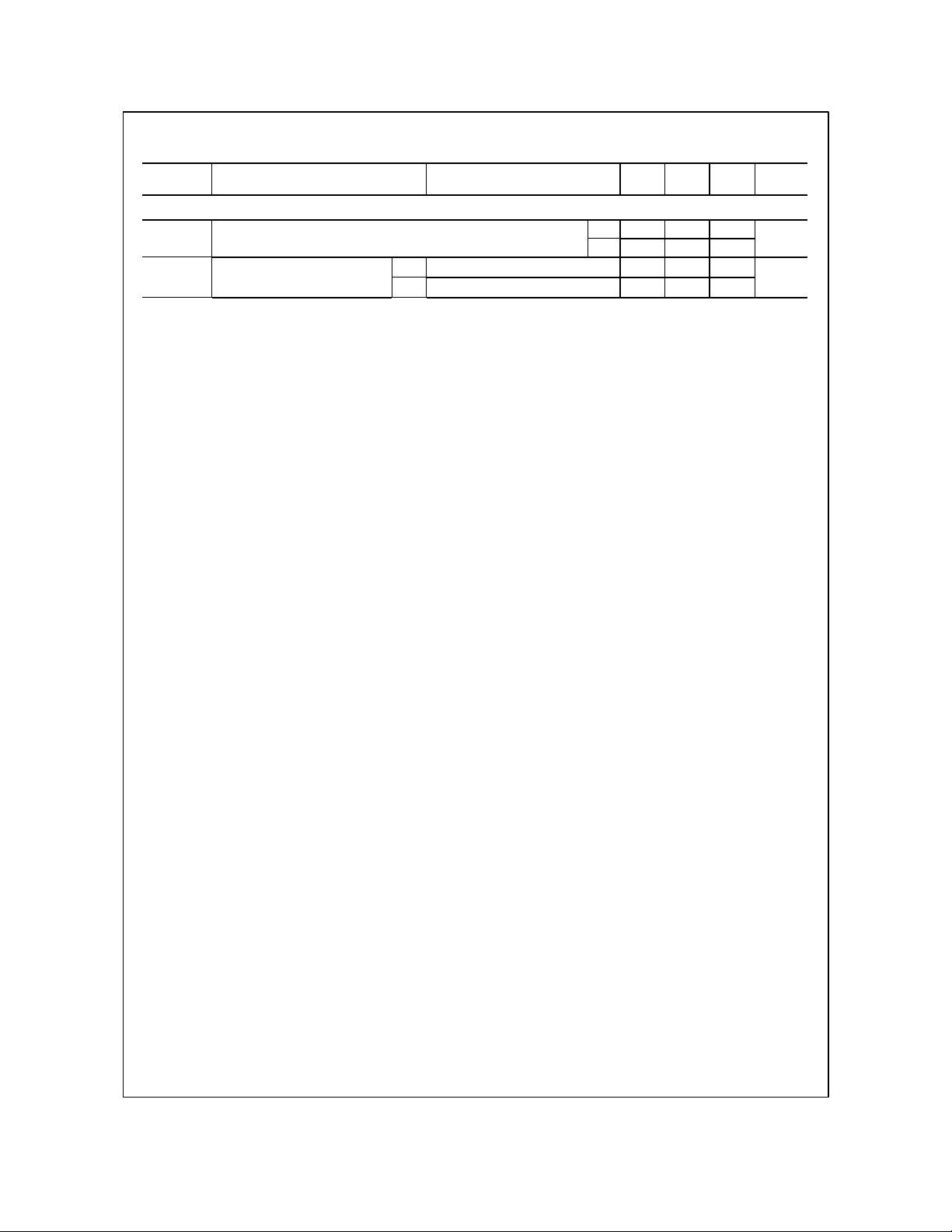
Electrical Characteristics T
FDG6332C
= 25°C unless otherwise noted
A
Symbol Parameter Test Conditions Min Typ Max Units
Drain–Source Diode Characteristics and Maximum Ratings
I
S
Maximum Continuous Drain–Source Diode Forward Current
Q1
Q2
= 0 V, IS = 0.25 A (Note 2)
V
SD
Drain–Source Diode Forward
Voltage
Notes:
1. R
is the sum of the junction-to-case and case-to-ambient thermal resistance where the case thermal reference is defined as the solder mounting surface of
θJA
the drain pins. R
PCB in a still air environment.
2. Pulse Test: Pulse Width < 300µs, Duty Cycle < 2.0%
is guaranteed by design while R
θJC
is determined by the user's board design. R
θJA
Q1
Q2
V
GS
V
= 0 V, IS = –0.25 A (Note 2)
GS
–0.77 –1.2
= 415°C/W when mounted on a minimum pad of FR-4
θJA
0.25
–0.25
0.74 1.2
A
V
FDG6332C Rev C2 (W)
 Loading...