

Fairchild Semiconductor FDG6323L Datasheet
FDG6323L
Integrated Load Switch
General Description Features
V
=0.2V @ VIN=5V, IL=0.36A. R
ROP
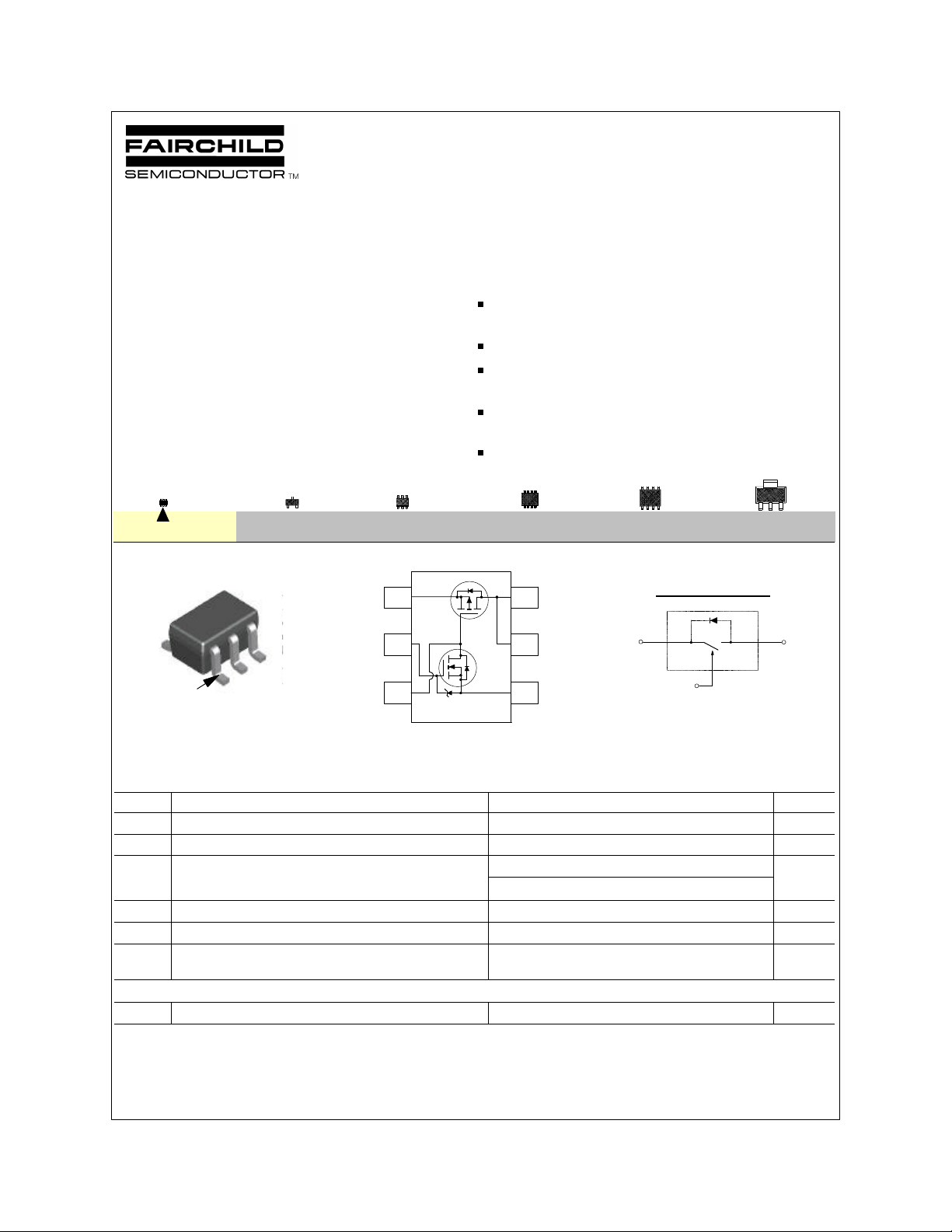
This device is particularly suited for compact
power management in portable electronic
equipment where 2.5V to 8V input and 0.6A
output current capability are needed. This load
switch integrates a small N-Channel power
MOSFET (Q1) which drives a large P-Channel
power MOSFET (Q2) in one tiny SC70-6
package.
D
V
=0.2V @ VIN=2.5V, IL=0.27A. R
DROP
Very small package outline SC70-6.
Control MOSFET (Q1) includes Zener protection for ESD
ruggedness (>6KV Human Body Model).
High density cell design for extremely low
on-resistance.
Compact industry standard SC70-6 surface mount package.
March 1999
= 0.55Ω
(ON)
= 0.75Ω.
(ON)
SC70-6
SOT-23
SuperSOTTM-6
SuperSOTTM-8
SO-8
SOT-223
V , C
3
2
Q1
1
OUT
V , C
OUT
R
2
1
1
.23
1
pin
SC70-6
Absolute Maximum Ratings T
V , R
4
1
IN
Q2
V
ON/OFF
5
R , C
6
1
1
See Application Circuit
= 25°C unless otherwise noted
A
Symbol Parameter FDG6323L Units
V
V
I
L
IN
ON/OFF
Input Voltage Range 2.5 - 8 V
On/Off Voltage Range 1.5 - 8 V
Load Current - Continuous (Note 1) 0.6 A
- Pulsed (Note 1 & 3) 1.8
P
D
TJ,T
Maximum Power Dissipation (Note 2) 0.3 W
Operating and Storage Temperature Range -55 to 150 °C
STG
ESD Electrostatic Discharge Rating MIL-STD-883D Human Body
Model (100pf/1500Ohm)
THERMAL CHARACTERISTICS
R
JA
θ
Thermal Resistance, Junction-to-Ambient (Note 2) 415 °C/W
EQUIVALENT APPLICATION
V
DROP
+
IN
ON/OFF
-
6 kV
OUT
© 1999 Fairchild Semiconductor Corporation
FDG6323L Rev.C

Electrical Characteristics (T
= 25°C unless otherwise noted)
A
Symbol Parameter Conditions Min Typ Max Units
OFF CHARACTERISTICS
I
FL
Forward Leakage Current VIN = 8 V, V
= 0 V 1 µA
ON/OFF
ON CHARACTERISTICS (Note 3)
V
DROP
R
(ON)
Conduction Voltage Drop VIN = 5 V, V
VIN = 2.5 V, V
= 3.3 V, IL = 0.36 A 0.14 0.2 V
ON/OFF
= 3.3 V, IL = 0.27 A
ON/OFF
0.15 0.2
Q2 - Static On-Resistance VGS = -5 V, ID = -0.6 A 0.41 0.55
VGS = -2.5 V, ID = -0.5 A 0.58 0.75
I
L
Notes:
1. Range of Vin can be up to 8V, but R1 and R2 must be scaled such that VGS of Q2 does not exceed -8V.
2. R
θ
R
θ
3. Pulse Test: Pulse Width < 300µs, Duty Cycle < 2.0%
Load Current V
is the sum of the junction-to-case and case-to-ambient thermal resistance where the case thermal reference is defined as the solder mounting surface of the drain pins.
JA
is guaranteed by design while R
JC
is determined by the user's board design.
CA
θ
= 0.2 V, VIN = 5 V, V
DROP
V
= 0.2 V, VIN = 2.5 V, V
DROP
= 3.3 V 0.36 A
ON/OFF
= 3.3 V 0.27
ON/OFF
FDG6323L Load Switch Application
APPLICATION CIRCUIT
Ω
Q2
IN
R1
Q1
ON/OFF
R2
External Component Recommendation
R1 is required to turn Q2 off.
R2 is optional for Slew Rate Control.
For Co ≤ 1uF applications:
First select R2,100 - 1KΩ, for Slew Rate control.
Then select R1 such that R1/R2 ratio maintains between 10 - 100.
OUT
C1
Co
LOAD
FDG6323L Rev.C

Typical Electrical Characteristics (T
= 25 OC unless otherwise noted )
A
1.5
V = 5V
IN
V = 1.5 - 8V
ON/OFF
1.2
PW =300us, D≤ 2%
0.9
DROP
0.6
V ,(V)
T = 125°C
J
T = 25°C
J
0.3
0
0 0.4 0.8 1.2 1.6 2
I ,(A)
L
Figure 1. Conduction Voltage Drop
Variation with Load Current.
1
0.8
0.6
(ON)
R ,(Ohm)
0.4
0.2
0 2 4 6 8 10
V , (V)
IN
I = 1A
L
V = 1.5 - 8V
ON/OFF
PW =300us, D≤ 2%
T = 125°C
J
T = 25°C
J
1.5
T = 125°C
I , (A)
L
J
T = 25°C
J
V = 2.5V
IN
V = 1.5 - 8V
ON/OFF
PW =300us, D≤ 2%
1.2
0.9
DROP
0.6
V , (V)
0.3
0
0 0.4 0.8 1.2 1.6 2
Figure 2. Conduction Voltage Drop
Variation with Load Current.
Figure 3. On-Resistance Variation
with Input Voltage.
1
D = 0.5
0.5
0.2
0.2
0.1
0.1
0.05
0.02
0.01
r(t), NORMALIZED EFFECTIVE
0.005
TRANSIENT THERMAL RESISTANCE
0.002
0.05
0.02
0.01
Single Pulse
0.0001 0.001 0.01 0.1 1 10 100 200
Figure 4. Transient Thermal Response Curve.
Thermal characterization performed using the conditions described in Note 2.
Transient thermal response will change depending on the circuit board design.
t , TIME (sec)
1
R (t) = r(t) * R
JA
θ
R =415
JA
θ
P(pk)
t
1
t
2
T - T = P * R (t)
J
A
Duty Cycle, D = t / t
°C/W
JA
θ
1 2
JA
θ
FDG6323L Rev.C
 Loading...