

Fairchild Semiconductor FDG6322C Datasheet
February 1998
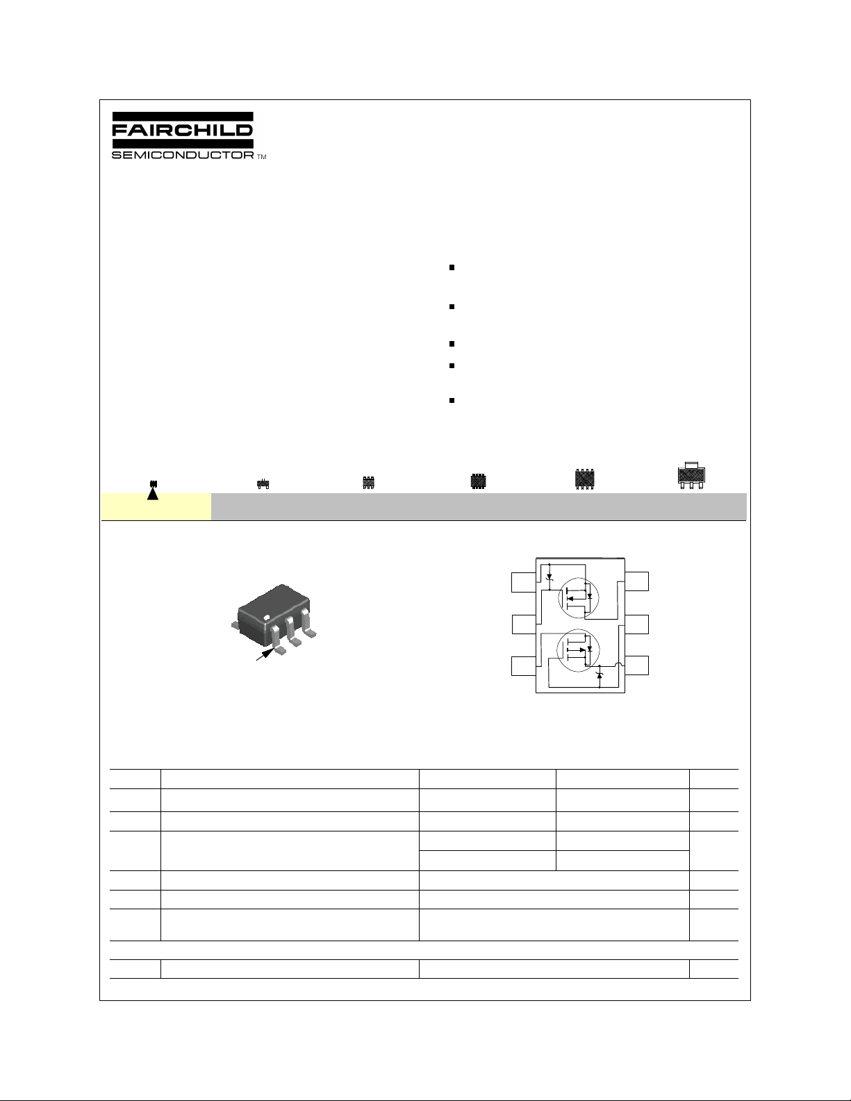
FDG6322C
Dual N & P Channel Digital FET
General Description Features
These dual N & P-Channel logic level enhancement mode
field effect transistors are produced using Fairchild's
proprietary, high cell density, DMOS technology. This very
high density process is especially tailored to minimize
on-state resistance. This device has been designed
especially for low voltage applications as a replacement for
bipolar digital transistors and small signal MOSFETs. Since
bias resistors are not required, this dual digital FET can
replace several different digital transistors, with different bias
resistor values.
SC70-6
SOT-23
SuperSOT
S2
G2
D1
D2
SC70-6
Mark: .22
pin
1
S1
G1
N-Ch 0.22 A, 25 V, R
R
P-Ch -0.41 A,-25V, R
R
DS(ON)
= 4.0 Ω @ VGS= 4.5 V,
DS(ON)
= 5.0 Ω @ VGS= 2.7 V.
DS(ON)
= 1.1 Ω @ VGS= -4.5V,
DS(ON)
= 1.5 Ω @ VGS= -2.7V.
Very small package outline SC70-6.
Very low level gate drive requirements allowing direct
operation in 3 V circuits (V
GS(th)
< 1.5 V).
Gate-Source Zener for ESD ruggedness
(>6kV Human Body Model).
TM
-6
SOT-8
1
2
3
SO-8
SOIC-14
66
Q1
5
Q2
4
Absolute Maximum Ratings T
Symbol Parameter N-Channel P-Channel Units
V
DS
V
GSS
I
D
Drain-Source Voltage 25 -25 V
S
Gate-Source Voltage 8 -8 V
Drain Current - Continuous 0.22 -0.41 A
= 25oC unless other wise noted
A
- Pulsed 0.65 -1.2
P
D
T
J,TSTG
ESD Electrostatic Discharge Rating MIL-STD-883D
Maximum Power Dissipation (Note 1) 0.3 W
Operating and Storage Temperature Range -55 to 150 °C
6 kV
Human Body Model (100pf / 1500 Ohm)
THERMAL CHARACTERISTICS
R
JA
θ
© 1998 Fairchild Semiconductor Corporation
Thermal Resistance, Junction-to-Ambient (Note1) 415 °C/W
FDG6322C Rev.F
DMOS Electrical Characteristics (T
= 25 OC unless otherwise noted )
A
Symbol Parameter Conditions
OFF CHARACTERISTICS
BV
DSS
Drain-Source Breakdown Voltage VGS = 0 V, ID = 250 µA N-Ch 25 V
VGS = 0 V, ID = -250 µA P-Ch -25
∆BV
DSS
Breakdown Voltage Temp. Coefficient ID = 250 µA, Referenced to 25 oC N-Ch 25 mV/oC
/∆T
J
ID = -250 µA, Referenced to 25 oC P-Ch -22
I
DSS
I
DSS
I
GSS
Zero Gate Voltage Drain Current V
= 20 V, VGS= 0 V, N-Ch 1 µA
DS
Zero Gate Voltage Drain Current VDS =-20 V, V
Gate - Body Leakage Current VGS = 8 V, V
VGS = -8 V, V
ON CHARACTERISTICS (Note 2)
V
GS(th)
Gate Threshold Voltage VDS = VGS, ID = 250 µA N-Ch 0.65 0.85 1.5 V
VDS = VGS, ID = -250 µA P-Ch -0.65 -0.82 -1.5
∆V
GS(th)
Gate Threshold Voltage Temp. Coefficient ID = 250 µA, Referenced to 25 o C N-Ch -2.1 mV/ oC
/∆T
J
ID= -250 µA, Referenced to 25 o C P-Ch 2.1
R
DS(ON)
Static Drain-Source On-Resistance VGS = 4.5 V, ID = 0.22 A N-Ch 2.6 4
VGS = 2.7 V, ID = 0.19 A 3.7 5
VGS = -4.5 V, ID = -0.41 A P-Ch 0.85 1.1
VGS = -2.7 V, ID = -0.25 A 1.15 1.5
I
D(ON)
On-State Drain Current VGS = 4.5 V, VDS = 5 V N-Ch 0.22 A
VGS = -4.5 V, VDS = -5 V P-Ch -0.41
g
FS
Forward Transconductance VDS = 5 V, ID= 0.22 A N-Ch 0.2 S
VDS = -5 V, ID = -0.5 A P-Ch 0.9
DYNAMIC CHARACTERISTICS
C
iss
C
oss
Input Capacitance N-Channel N-Ch 9.5 pF
V
= 10 V, V
DS
Output Capacitance f = 1.0 MHz N-Ch 6
P-Channel P-Ch 34
C
rss
Reverse Transfer Capacitance V
= -10 V, VGS = 0 V, N-Ch 1.3
DS
f = 1.0 MHz P-Ch 10
Min Typ Max Units
Type
TJ = 55°C 10
= 0 V, P-Ch -1 µA
GS
TJ = 55°C -10
= 0 V N-Ch 100 nA
DS
= 0 V P-Ch -100 nA
DS
TJ =125°C 5.3 7
TJ =125°C 1.2 1.9
= 0 V, P-Ch 62
GS
Ω
FDG6322C Rev.F
Electrical Characteristics (continued)
SWITCHING CHARACTERISTICS (Note 2)
Symbol Parameter Conditions
t
D(on)
Turn - On Delay Time N-Channel N-Ch 5 10 nS
Type
VDD = 5 V, ID = 0.5 A, P-Ch 7 15
t
r
Turn - On Rise Time
VGS = 4.5 V, R
= 50 Ω
GEN
N-Ch 4.5 10 nS
P-Ch 8 16
t
D(off)
Turn - Off Delay Time P-Channel N-Ch 4 8 nS
VDD = -5 V, ID = -0.5 A, P-Ch 55 80
t
f
Turn - Off Fall Time
VGS = -4.5 V, R
GEN
= 50 Ω
N-Ch 3.2 7 nS
P-Ch 35 60
Q
g
Total Gate Charge N-Channel N-Ch 0.29 0.4 nC
VDS= 5 V, ID = 0.22 A, P-Ch 1.1 1.5
Q
gs
Gate-Source Charge VGS = 4.5 V N-Ch 0.12 nC
P- Channel P-Ch 0.31
Q
gd
Gate-Drain Charge VDS = -5 V, ID = -0.41 A, N-Ch 0.03 nC
VGS = -4.5 V P-Ch 0.29
DRAIN-SOURCE DIODE CHARACTERISTICS AND MAXIMUM RATINGS
I
S
Maximum Continuous Drain-Source Diode Forward Current N-Ch 0.25 A
P-Ch -0.25
V
SD
Notes:
1. R
by design while R
2. Pulse Test: Pulse Width < 300µs, Duty Cycle < 2.0%.
Drain-Source Diode Forward Voltage VGS = 0 V, IS = 0.5 A
VGS = 0 V, IS = -0.5 A
is the sum of the junction-to-case and case-to-ambient thermal resistance where the case thermal reference is defined as the solder mounting surface of the drain pins. R
JA
θ
is determined by the user's board design. R
CA
θ
= 415OC/W on minimum mounting pad on FR-4 board in still air.
JA
θ
(Note 2) N-Ch 0.8 1.2 V
(Note 2) P-Ch -0.85 -1.2
Min Typ Max Units
is guaranteed
JC
θ
FDG6322C Rev.F
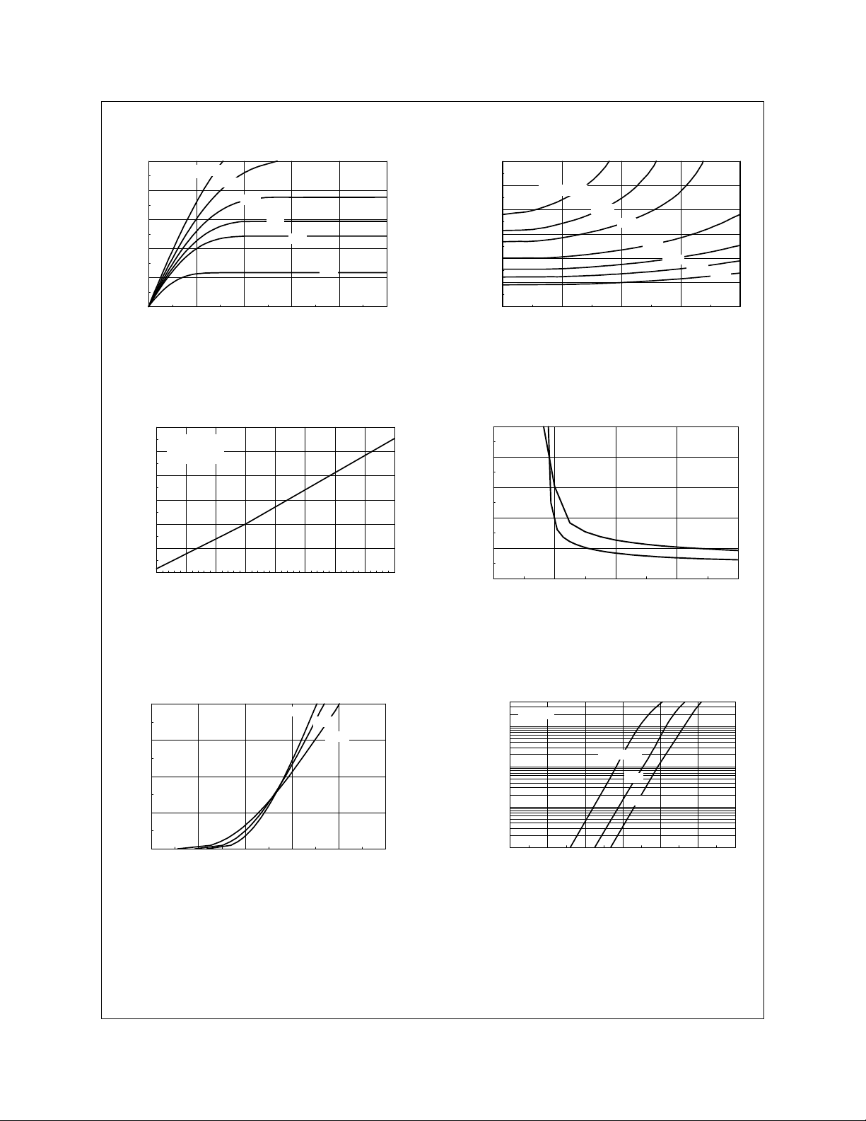
Typical Electrical Characteristics: N-Channel
0.5
0.4
0.3
0.2
0.1
D
I , DRAIN-SOURCE CURRENT (A)
V =4.5V
GS
3.5V
3.0V
0
0 1 2 3 4 5
V , DRAIN-SOURCE VOLTAGE (V)
DS
Figure 1. On-Region Characteristics.
1.8
I = 0.22A
D
1.6
V = 4.5V
GS
1.4
1.2
1
DS(ON)
R , NORMALIZED
0.8
DRAIN-SOURCE ON-RESISTANCE
0.6
-50 -25 0 25 50 75 100 125 150
T , JUNCTION TEMPERATURE (°C)
J
4.5
4
V = 2.5V
GS
2.7V
3.0V
3.5V
3
DS(ON)
R , NORMALIZED
2.5
DRAIN-SOURCE ON-RESISTANCE
0 0.1 0.3 0.4
I , DRAIN CURRENT (A)
D
4.0V
Figure 2. On-Resistance Variation with
Drain Current and Gate Voltage.
20
16
12
8
T =125°C
4
DS(ON)
R , ON-RESISTANCE(OHM)
0
1 2 3 4 5
V ,GATE TO SOURCE VOLTAGE (V)
GS
A
I = 0.10A
25°C
4.5V
D
5.0V
Figure 3. On-Resistance Variation
with Temperature.
0.2
V = 5V
DS
0.15
0.1
0.05
D
I , DRAIN CURRENT (A)
0
0.5 1 1.5 2 2.5 3
V , GATE TO SOURCE VOLTAGE (V)
GS
Figure 5. Transfer Characteristics.
T = -55°C
J
25°C
125°C
Figure 4. On-Resistance Variation with
Gate-to-Source Voltage.
V = 0V
0.1
0.01
J
-55°C
S
I , REVERSE DRAIN CURRENT (A)
0.0001
0 0.2 0.6 0.8 1.2
V , BODY DIODE FORWARD VOLTAGE (V)
SD
Figure 6 Voltage
tion with Source Current
and Temperature.
FDG6322C Rev.F
 Loading...