

Fairchild Semiconductor FDG361N Datasheet
FDG361N
N-Channel 100V Specified PowerTrenchMOSFET
FDG361N
August 2001
General Description
These N-Channel 100V specified MOSFETs are
produced using Fairchild Semiconductor's advanced
PowerTrench process that has been especially tailored
to minimize on-state resistance and yet maintain low
gate charge for superior switching performance.
These devices have been designed to offer exceptional
power dissipation in a very small footprint for
applications where the bigger more expensive SO-8
and TSSOP-8 packages are impractical.
Features
•
0.6 A, 100 V. R
R
= 500 mΩ @ VGS = 10 V
DS(ON)
= 550 mΩ @ VGS = 6.0 V
DS(ON)
• Low gate charge (3.7nC typical)
• Fast switching speed
• High performance trench technology for extremely
low R
DS(ON)
Applications
• Load switch
• Battery protection
• Power management
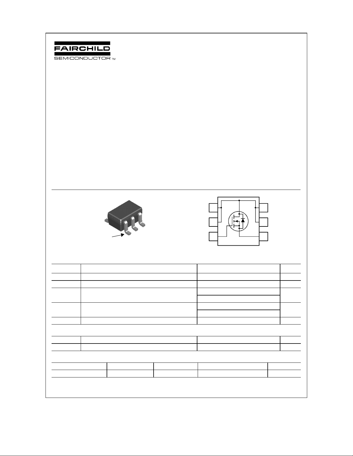
S
D
D
1
2
6
5
G
Pin 1
SC70-6
Absolute Maximum Ratings T
D
D
=25oC unless otherwise noted
A
3
4
Symbol Parameter Ratings Units
V
DSS
V
GSS
I
D
P
D
TJ, T
STG
Drain-Source Voltage 100 V
Gate-Source Voltage
Drain Current – Continuous (Note 1a) 0.6 A
– Pulsed 2.0
Power Dissipation for Single Operation (Note 1a) 0.42
(Note 1b)
Operating and Storage Junction Temperature Range
±20
0.38
−55 to +150 °C
V
W
Thermal Characteristics
R
θJA
R
θJA
Thermal Resistance, Junction-to-Ambient (Note 1a) 300
Thermal Resistance, Junction-to-Ambient (Note 1b) 333
Package Marking and Ordering Information
Device Marking Device Reel Size Tape width Quantity
.61 FDG361N 7’’ 8mm 3000 units
2001 Fairchild Semiconductor Corporation
°C/W
°C/W
FDG361N Rev C(W)

FDG361N
Electrical Characteristics T
= 25°C unless otherwise noted
A
Symbol Parameter Test Conditions Min Typ Max Units
Off Characteristics
BV
DSS
∆BVDSS
∆T
J
I
DSS
I
GSSF
I
GSSR
Drain–Source Breakdown Voltage
Breakdown Voltage Temperature
Coefficient
= 0 V, ID = 250 µA
V
GS
I
= 250 µA,Referenced to 25°C
D
Zero Gate Voltage Drain Current VDS = 80 V, VGS = 0 V 10
Gate–Body Leakage, Forward VGS = 20 V, VDS = 0 V 100 nA
Gate–Body Leakage, Reverse VGS = –20 V, VDS = 0 V –100 nA
100 V
105
mV/°C
On Characteristics (Note 2)
V
GS(th)
∆VGS(th)
∆T
J
R
DS(on)
I
D(on)
g
FS
Gate Threshold Voltage
Gate Threshold Voltage
Temperature Coefficient
Static Drain–Source
On–Resistance
= VGS, ID = 250 µA
V
DS
I
= 250 µA,Referenced to 25°C
D
V
= 10 V, ID = 0.6 A
GS
= 6 V, ID = 0.6 A
V
GS
= 10 V, ID = 0.6 A, TJ = 125°C
V
GS
On–State Drain Current VGS = 10 V, VDS = 10 V 2 A
Forward Transconductance VDS = 5V, ID = 0.6 A 3.6 S
22.64 V
–5
370
396
685
500
550
976
mV/°C
mΩ
Dynamic Characteristics
C
iss
C
oss
C
rss
Input Capacitance 153 pF
Output Capacitance 5 pF
Reverse Transfer Capacitance
= 50 V, V
V
DS
f = 1.0 MHz
GS
= 0 V,
1pF
Switching Characteristics (Note 2)
t
t
t
t
Q
Q
Q
d(on)
r
d(off)
f
g
gs
gd
Turn–On Delay Time 8 16 ns
Turn–On Rise Time 4 8 ns
= 50 V, ID = 1 A,
V
DD
= 10 V, R
V
GS
GEN
= 6 Ω
Turn–Off Delay Time 11 20 ns
Turn–Off Fall Time
Total Gate Charge 3.7 5 nC
Gate–Source Charge 0.8 nC
V
= 50 V, ID = 0.6 A,
DS
= 10 V
V
GS
Gate–Drain Charge
612ns
1nC
Drain–Source Diode Characteristics and Maximum Ratings
I
S
V
SD
Notes:
1. R
is the sum of the junction-to-case and case-to-ambient thermal resistance where the case thermal reference is defined as the solder mounting surface of
θJA
the drain pins. R
Maximum Continuous Drain–Source Diode Forward Current 0.4 A
Drain–Source Diode Forward
VGS = 0 V, IS = 0.4 A (Note 2) 0.8 1.2 V
Voltage
is guaranteed by design while R
θJC
is determined by the user's board design.
θCA
µA
a) 300°C/W when
2. Pulse Test: Pulse Width < 300µs, Duty Cycle < 2.0%
mounted on a 1in
of 2 oz copper.
2
pad
b) 333°C/W when mounted
on a minimum pad of 2 oz
copper.
FDG361N Rev C(W)
 Loading...