

Fairchild Semiconductor FDG316P Datasheet
FDG316P
P-Channel Logic Level PowerTrench
MOSFET
FDG316P
December 2001
General Description
This P-Channel Logic Level MOSFET is produced using
Fairchild Semiconductor's advanced PowerTrench
process that has been especially tailored to minimize
on-state resistance and yet maintain superior
switching performance.
These devices are well suited for low voltage and
battery powered applications where low in-line power
loss and fast switching are required.
Applications
• DC/DC converter
• Load switch
• Power Management
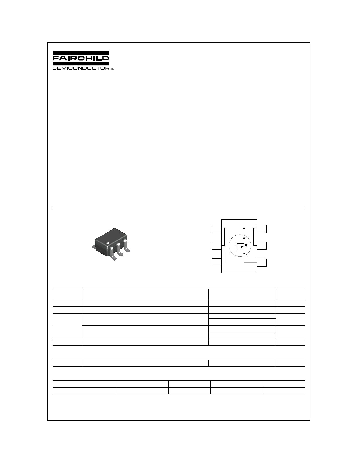
S
D
D
G
SC70-6
D
D
Features
• -1.6 A, -30 V. R
R
= 0.19 Ω @ V
DS(ON)
= 0.30 Ω @ V
DS(ON)
= -10 V
GS
= -4.5 V.
GS
• Low gate charge (3.5nC typical).
• High performance trench technology for extremely low
R
DS(ON)
.
• Compact industry standard SC70-6 surface mount
package.
1
2
3
3
6
5
4
Absolute Maximum R atings
TA = 25°C unless otherwise noted
Symbol Parameter Ratings Units
V
DSS
V
GSS
I
D
P
D
TJ, T
stg
Drain-Source Voltage -30 V
Gate-Source Voltage ±
Drain Current - Continuous
- Puls e d -6
Power Dissipation for Single Operation
Operating and Storage Junction Tem perature Range -55 to +150 °
(Note 1a)
(Note 1a)
(Note 1b)
20
-1.6 A
0.75 W
0.48
Thermal Characteristics
R
JA
θ
Thermal Resistance, Junction-to-Amb ient
(Note 1b)
260
Package Marking and Ordering Information
Device Marking Device Reel Size Tape Width Quantity
.
36
2001 Fairchild Semiconductor Corporation
FDG316P 7’’ 8mm 3000 units
V
C
°C/W
FDG316P Rev. D
FDG316P
Electrical Characteristics T
= 25°C unless otherwise noted
A
Symbol Parameter Test Conditions Min Typ Max Units
Off Characteristics
BV
∆
∆
I
DSS
I
GSS
I
GSS
BV
DSS
T
DSS
J
Drain-Source Breakdown Voltage
Breakdown Voltage Temperature
Coefficient
= 0 V, ID = -250 µA
V
GS
= -250 µA, Referenced to 25°C
I
D
Zero Gate Voltage Drain Current VDS = -24 V, VGS = 0 V -1
Gate-Body Leakage Forward VGS = 16 V, VDS = 0 V 100 nA
Gate-Body Leakage Reverse VGS = -16 V, VDS = 0 V -100 nA
-30 V
-34
mV/°C
µ
On Characteristics (Note 2)
V
∆
∆
R
I
D(on)
g
GS(th)
V
GS(th)
T
DS(on)
FS
Gate Threshold Voltage
Gate Threshold Voltage
J
Temperature Coeffic i ent
Static Drain-Source
On-Resistance
= VGS, ID = -250 µA
V
DS
= -250 µA, Referenced to 25°C
I
D
VGS = -10 V, ID = -1.6 A
V
= -10 V, ID = -1.6 A,TJ =125°C
GS
V
= -4.5 V, ID = -1.3 A
GS
On-State Drain Current VGS = -4.5 V, VDS = -5 V -3 A
Forward Transconductance VDS = -5 V, ID = -0.5 A 3 S
-1 -1.6 -3 V
3.5
0.16
0.22
0.23
mV/°C
0.19
0.31
0.30
Ω
Dynamic Characteristics
C
iss
C
oss
C
rss
Input Capacitance 165 pF
Output Capacitance 60 pF
Reverse Transfer Capacitanc e
V
= -15 V, VGS = 0 V,
DS
f = 1.0 MHz
25 pF
A
Switching Characteristics (Note 2)
t
t
t
t
Q
Q
Q
d(on)
r
d(off)
f
g
gs
gd
Turn-On Delay Time 8 20 ns
Turn-On Rise Time 9 20 ns
= -15 V, ID = -1 A,
V
DD
V
= -10 V, R
GS
GEN
= 6
Ω
Turn-Off Delay Time 14 30 ns
Turn-Off Fall Time
Total Gate Charge 3.5 5 nC
Gate-Source Charge 0.6 nC
V
= -15 V, ID = -1.6 A,
DS
= -10 V
V
GS
Gate-Drain Charge
Drain-Source Diode Characteristics and Maximum Ratings
I
S
V
SD
Notes:
1. R
is the sum of the junction-to-case and case-to-ambient thermal resistance where the case thermal reference is defined as the solder mounting surface
θJA
of the drain pins. R
a) 170°C/W when mounted on a 1 in2 pad of 2oz copper.
b) 260°C/W when mounted on a minimum pad.
2. Pulse T est: Pulse Width ≤ 300 µs, Duty Cycle ≤ 2.0%
Maximum Continuous Drain-Source Diode Forward Current -0.42 A
Drain-Source Diode Forward
VGS = 0 V, IS = -0.42 A (Note 2) 0.75 -1.2 V
Voltage
is guaranteed by design while R
θJC
is determined by the user's board design.
θCA
210ns
0.8 nC
FDG316P Rev. D
 Loading...