

Fairchild Semiconductor FDG314P Datasheet
FDG314P
Digital FET, P-Channel
FDG314P
July 2000
General Description
This P-Channel enhancement mode field effect
transistor is produced using Fairchild Semiconductor’s
proprietary, high cell density, DMOS technology. This
very high density process is tailored to minimize onstate resistance at low gate drive conditions. This
device is designed especially for battery power
applications such as notebook computers and cellular
phones. This device has excellent on-state resistance
even at gate drive voltages as low as 2.5 volts.
Applications
• Power Management
• Load switch
• Signal switch
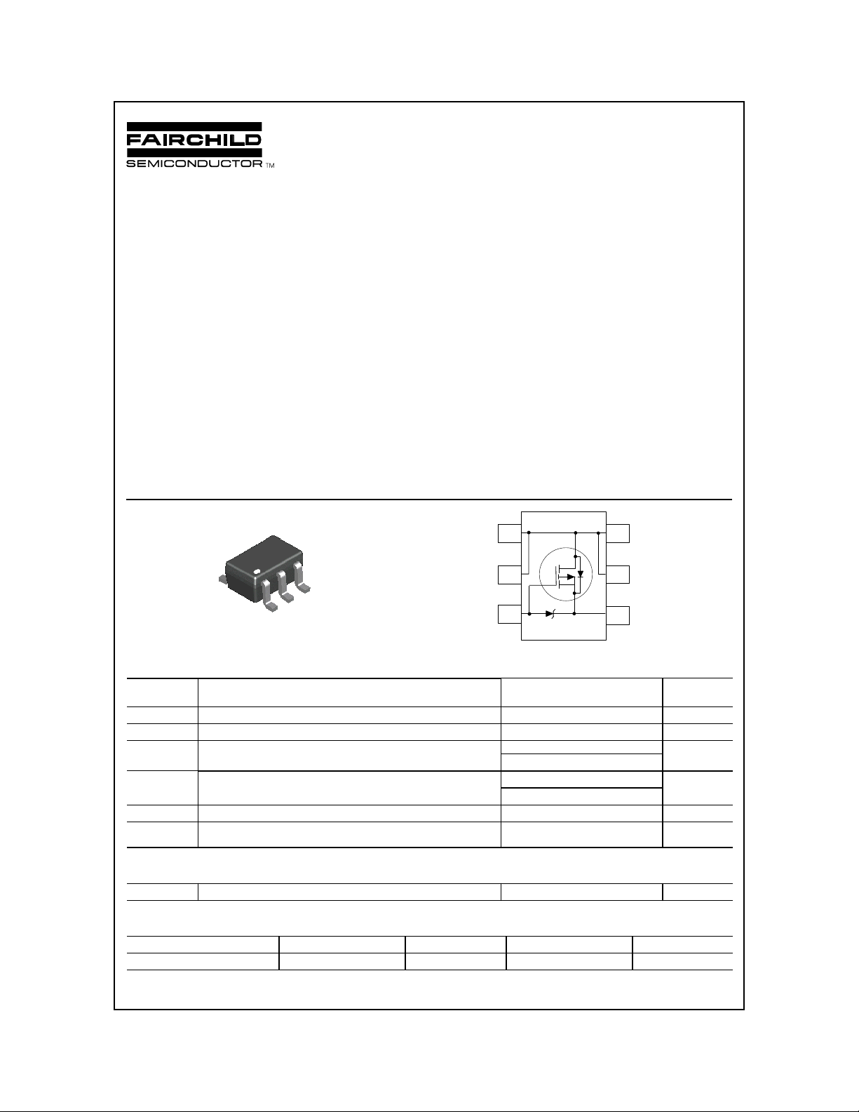
S
D
D
G
SC70-6
Absolute Maximum Ratings
D
D
TA = 25°C unless otherwise noted
Features
• -0.65 A, -25 V. R
R
= 1.1 Ω @ V
DS(ON)
= 1.5 Ω @ V
DS(ON)
= -4.5 V
GS
= -2.7 V.
GS
• Very low gate drive requirements allowing direct
operation in 3V cirucuits (V
GS(th)
<1.5 V).
• Gate-Source Zener for ESD ruggedness
(>6 kV Human Body Model).
• Compact industry standard SC70-6 surface mount
package.
1
2
3
3
6
5
4
Symbol Parameter Ratings Units
V
DSS
V
GSS
I
D
P
D
TJ, T
stg
ESD Electrostatic Discharge Rating MIL-STD-883D
Drain-Source Voltage -25 V
Gate-Source Voltage
Drain Current - Continuous (Note 1a) -0.65 A
- Pulsed -1.8
Power Dissipation for Single Operation
Operating and Storage Junction Temperature Range -55 to +150 °
Human Body Model (100pf/1500 Ohm )
(Note 1a)
(Note 1b)
±
8V
0.75 W
0.48
6.0
Thermal Characteristics
R
JA
θ
Thermal Resistance, Junction-to-Am bient (Note 1b) 260
Package Marking and Ordering Information
Device Marking Device Reel Size Tape Width Quantity
.
14
2000 Fairchild Semiconductor International
FDG314P 7’’ 8mm 3000 units
C
kV
°
C/W
FDG314P Rev.C
FDG314P
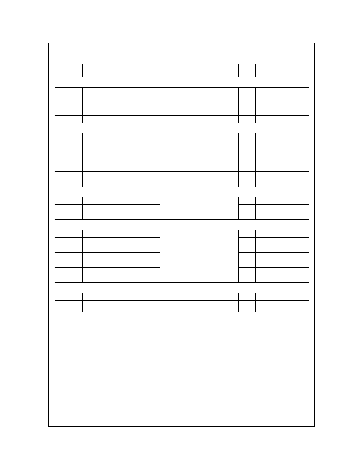
Electrical Characteristics T
= 25°C unless otherwise noted
A
Symbol Parameter Test Conditions Min Typ Max Units
Off Characteristics
BV
∆
∆
I
DSS
I
GSS
BV
DSS
T
DSS
J
Drain-Source Breakdown Voltage
Breakdown Voltage Temperature
Coefficient
V
= 0 V, ID = -250 µA
GS
ID = -250 µA, Referenced to 25°C
-25 V
-19
mV/°C
Zero Gate Voltage Drain Current VDS = -20 V, VGS = 0 V -1 µ
Gate-Body Leakage Current VGS = -8 V, VDS = 0 V -100 nA
On Characteristics (Note 2)
V
∆
∆
R
I
D(on)
g
GS(th)
V
GS(th)
T
DS(on)
FS
J
Gate Threshold Voltage
Gate Threshold Voltage
Temperature Coefficient
Static Drain-Source
On-Resistance
V
= VGS, ID = -250 µA
DS
ID = -250 µA, Referenced to 25°C
V
= -4.5 V, ID = -0.5 A
GS
V
= -4.5 V, ID = -0.5 A @ 125°C
GS
V
= -2.7 V, ID = -0.25 A
GS
-0.65 -0.72 -1.5 V
2
0.77
1.08
1.06
mV/°C
1.1
1.8
1.5
On-State Drain Current VGS = -4.5 V, VDS = -5 V -1 A
Forward Transconductance VDS = -4.5 V, ID = -0.5 A 0.9 S
Ω
Dynamic Characteristics
= -10 V, VGS = 0 V,
V
C
iss
C
oss
C
rss
Input Capacitance 63 pF
Output Capacitance 34 pF
Reverse Transfer Capacitance
DS
f = 1.0 MHz
10 pF
Switching Characteristics (Note 2)
= -6 V, ID = -0.5 A,
V
t
d(on)
t
r
t
d(off)
t
f
Q
Q
Q
Turn-On Delay Time 7 20 ns
Turn-On Rise Time 8 20 ns
Turn-Off Delay Time 55 110 ns
Turn-Off Fall Time
g
gs
gd
Total Gate Charge 1.1 1.5 nC
Gate-Source Charge 0.32 nC
Gate-Drain Charge
DD
V
= -4.5 V, R
GS
= -5 V, ID = -0.25 A,
V
DS
V
= -4.5 V
GS
GEN
= 50
Ω
35 70 ns
0.25 nC
A
Drain-Source Diode Characteristics and Maximum Ratings
I
S
V
SD
Notes:
1. R
is the sum of the junction-to-case and case-to-ambient thermal resistance where the case thermal reference is defined as the solder mounting surface
θJA
of the drain pins. R
a) 170°C/W when mounted on a 1 in2 pad of 2oz copper.
b) 260°C/W when mounted on a minimum mounting pad.
2. Pulse T est: Pulse Width ≤ 300 µs, Duty Cycle ≤ 2.0%
Maximum Continuous Drain-Source Diode Forward Current -0.42 A
Drain-Source Diode Forward
Voltage
is guaranteed by design while R
θJC
θCA
VGS = 0 V, IS = -0.42 A (Note 2)
is determined by the user's board design.
-0.85 -1 .2 V
FDG314P Rev.C
 Loading...