

Fairchild Semiconductor FDG313N Datasheet
FDG313N
Digital FET, N-Channel
General Description
This N-Channel enhancement mode field effect
transistor is produced using Fairchild's proprietary , high
cell density, DMOS technology. This very high density
process is especially tailored to minimize on-state
resistance. This device has been designed especially
for low voltage applications as a replacement for
bipolar digital transistor and small signal MOSFET.
Applications
• Load switch
• Battery protection
• Power management
July 2000
Features
• 0.95 A, 25 V. R
R
= 0.45 Ω @ V
DS(on)
= 0.60 Ω @ V
DS(on)
= 4.5 V
GS
= 2.7 V.
GS
• Low gate charge (1.64 nC typical)
• Very low level gate drive requirements allowing direct
operation in 3V circuits (V
GS(th)
< 1.5V).
• Gate-Source Zener for ESD ruggedness
(>6kV Human Body Model).
• Compact industry standard SC70-6 surface mount
package.
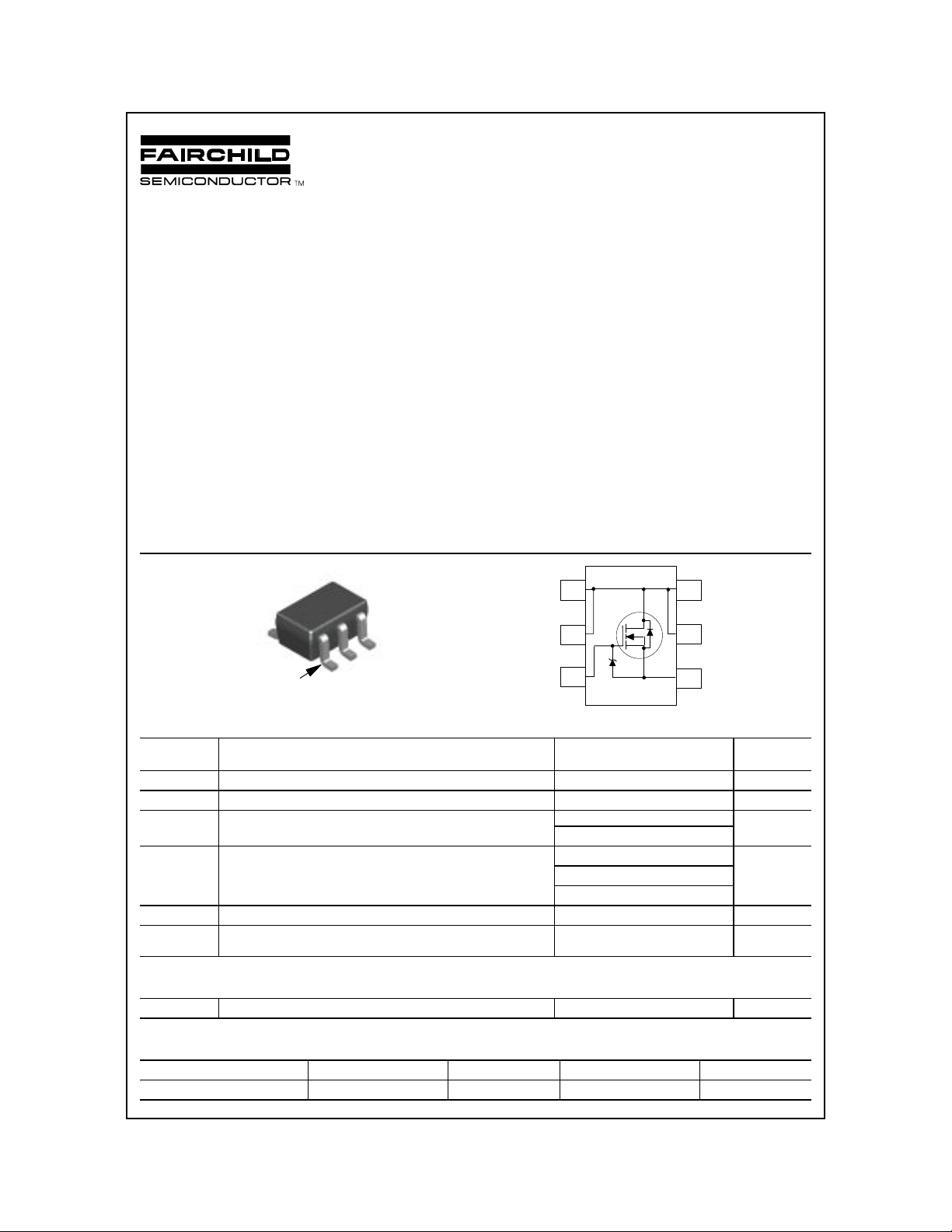
FDG313N
S
D
1
6
D
2
5
G
1
pin
SC70-6
Absolute Maximum Ratings
D
D
TA = 25°C unless otherwise noted
Symbol Parameter FDG313N Units
V
DSS
V
GSS
I
D
P
D
TJ, T
stg
ESD Electrostatic Di scharge Rating MIL-STD-883D
Drain-Source Voltage 25 V
Gate-Source Voltage
Drain Current - Continuous
- Pulsed 2
Power Dissipation for Si ngl e Operation
(Note 1b)
Operating and Storage Junction Temperature Range -55 to +150
Human Body Model (100pf / 1500 Ohm)
(Note 1a)
(Note 1a)
(Note 1c)
3
3
±
0.95 A
0.75 W
0.55
0.48
4
8V
C
°
6kV
Thermal Characteristics
R
JA
θ
Thermal Resistance, Junction-to-Ambient
(Note 1c)
260
C/W
°
Package Outlines and Ordering Information
Device Marking Device Reel Size Tape Width Quantity
13
.
1998 Fairchild Semiconductor Corporation
FDG313N 7’’ 8mm 3000 units
FDG313N Rev. C
FDG313N
yp
DMOS Electrical Characteristics
TA = 25°C unless otherwise noted
Symbol Parameter Test Conditions Min T
Off Characteristics
BV
DSS
BV
∆
T
∆
I
DSS
I
GSS
On Characteristics
V
GS(th)
GS(th)
V
∆
T
∆
R
DS(on)
I
D(on)
g
FS
Drain-Source Breakdown Voltage VGS = 0 V, ID = 250 µA25 V
Breakdown Voltage Temperature
DSS
Coefficient
J
ID = 250 µA, Referenced to 25°C30mV/
Zero Gate Voltage Drain Current VDS = 20 V, VGS = 0 V 1
Gate-Body Leakage Current VGS = 8 V, VDS = 0 V 100 nA
(Note 2)
Gate Threshold Voltage VDS = VGS, ID = 250 µA 0.65 0.8 1.5 V
Gate Threshold Voltage
Temperature Coefficient
J
Static Drain-Source
On-Resistance
ID = 250 µA, Referenced to 25°C-2mV/
VGS = 4.5 V, ID = 0.5 A
V
= 4.5 V, ID = 0.5 A @ 125°C
GS
V
= 2.7 V, ID = 0.2 A
GS
On-State Drain Current VGS = 4.5 V, VDS = 5 V 0.5 A
Forward Transconductance VDS = 5 V, ID = 0.5 A 1.5 S
Dynamic Characteristics
C
iss
C
oss
C
rss
Input Capacitance 50 pF
Output Capacitance 28 pF
Reverse Transfer Capacitance
Switching Characteristics
t
d(on)
t
r
t
d(off)
t
f
Q
Q
Q
g
gs
gd
Turn-On Delay Time 3 6 ns
Turn-On Rise Time 8.5 18 ns
Turn-Off Delay Time 17 30 ns
Turn-Off Fall Time
Total Gate Charge 1.64 2.3 nC
Gate-Source Charge 0.38 nC
Gate-Drain Charge
(Note 2)
V
= 10 V, VGS = 0 V,
DS
f = 1.0 MHz
= 6 V, ID = 0.5 A,
V
DD
V
= 4.5 V, R
GS
V
= 5 V, ID = 0.95 A,
DS
V
= 4.5 V
GS
GEN
= 50
Ω
Max Units
C
°
A
µ
C
°
0.35
0.45
0.53
0.76
0.45
0.6
9pF
13 25 ns
0.45 nC
Ω
Drain-Source Diode Characteristics and Maximum Ratings
I
S
V
SD
Notes:
1. R
θJA
drain pins. R
Scale 1 : 1 on letter size paper
2. Pulse Test: Pulse Width ≤ 300 µs, Duty Cycle ≤ 2.0%
Maximum Continuous Drain-Source Di ode Forward Current 0.6 A
copper.
(Note 2)
0.8 1.2 V
c) 260°C/W when
mounted on a minimum
pad of 2oz copper.
Drain-Source Diode Forward Voltage VGS = 0 V, IS = 0.6 A
is the sum of the junction-to-case and case-to-ambient resistance where the case thermal reference is defined as the solder mounting surface of the
is guaranteed by design while R
θJC
a) 170°C/W when
mounted on a 1 in
pad of 2oz copper.
is determined by the user's board design.
θJA
2
b) 225°C/W when
mounted on a half
of package sized 2oz.
FDG313N Rev. C
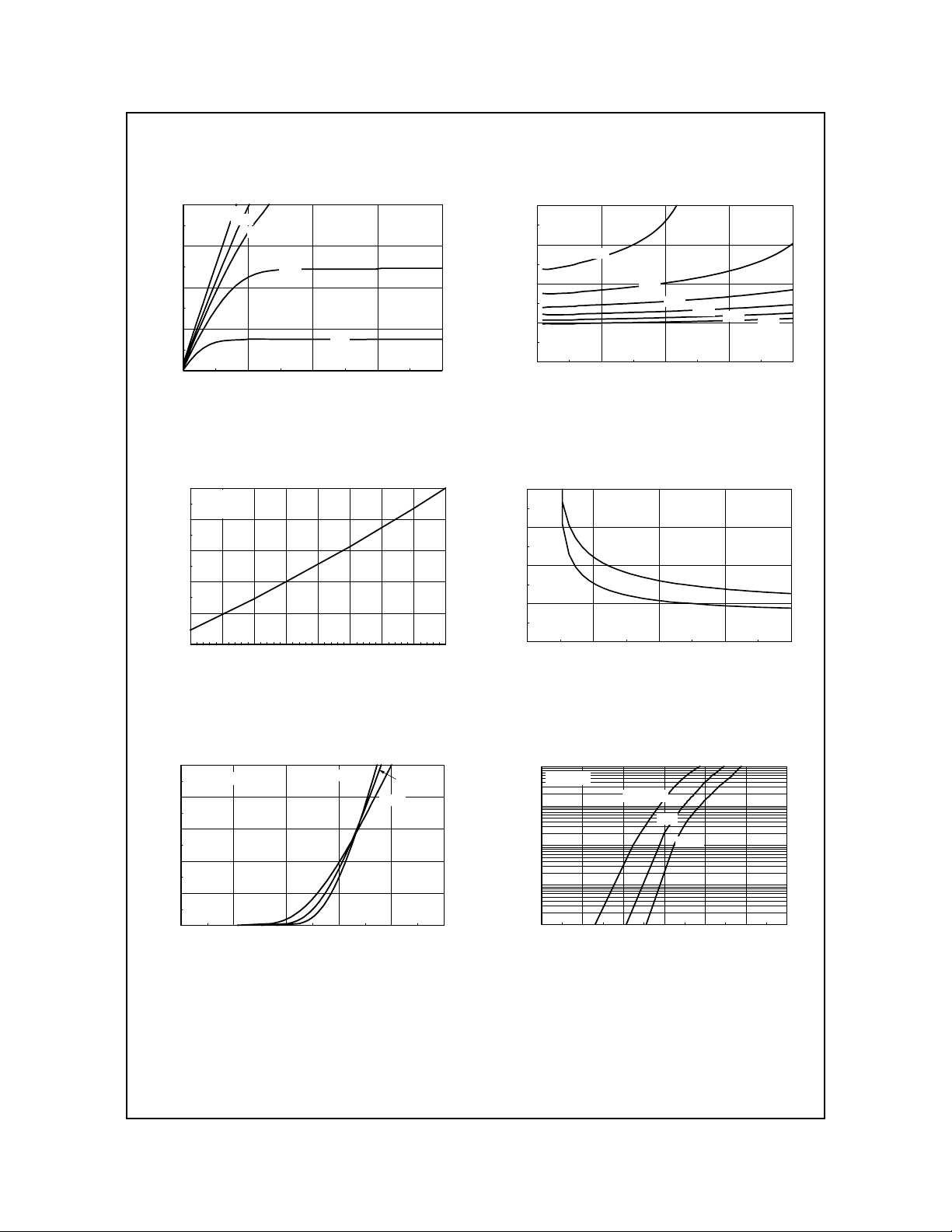
T ypical Characteristics
FDG313N
2
V = 4 .5V
GS
3.0V
2.5V
1.5
2.0V
1
0.5
D
I , DRAIN-SOURCE CURRENT (A)
0
01234
V , DRAIN-SOURCE VOLTAGE (V)
DS
1.5V
Figure 1. On-Region Characteristics.
1.6
I = 0.95 A
D
V = 4.5 V
GS
1.4
1.2
1
DS(ON)
R , NORMALIZED
0.8
DRAIN-SOURCE ON-RESISTANCE
0.6
-50 -25 0 25 50 75 100 125 150
T , JUNCTION TEMP ERATURE (°C)
J
2.5
2
V = 2.0V
GS
1.5
DS(ON)
1
R , NORMALIZED
DRAIN-SOURCE ON-RESISTANCE
0.5
00.511.52
2.5V
3.0V
3.5V
I , DRAIN CURRENT (A)
D
4.0V
4.5V
Figure 2. On-Resistance V ariation
with Drain Current and Gate V olt age.
1.6
I = 0. 5A
D
1.2
0.8
0.4
DS(ON)
R , ON-R ES IS TANCE (OHM)
0
12345
V , GATE TO SOURCE VOLTAGE (V)
GS
T = 125° C
A
T = 25°C
A
Figure 3. On-Resistance V ariation
with T emperature.
1
V = 5.0V
DS
0.8
0.6
0.4
D
I , DRAIN CURRENT (A)
0.2
0
00.511.522.5
V , GATE TO SOURCE VOLTAGE (V)
GS
T = -55°C
J
25°C
125°C
Figure 4. On-Resistance Variation
with Gate-to-Source Volt age.
1
V = 0V
GS
T = 125°C
0.1
0.01
0.001
S
I , REVERSE DRAIN CURRENT (A)
0.0001
00.20.40.60.811.2
V , BODY DIODE FORWARD VOLTAGE (V)
J
25°C
-55°C
SD
Figure 5. Transfer Characteristics. Figure 6. Body Diode Forward Voltage
Variation with Source Current
and Temperature.
FDG313N Rev. C
 Loading...