

Fairchild Semiconductor FAN5234 Datasheet
www.fairchildsemi.com
FAN5234
Mobile-Friendly PWM/PFM Controller
Features
• Wide input voltage range (2 to 24V) for Mobile systems
• Excellent dynamic response with Voltage Feed-Forward
and Average Current Mode control
• Lossless current sensing on low-side MOSFET or
precision over-current using sense resistor
• VCC Under-voltage Lockout
• Power-Good Signal
• Light load Hysteretic mode maximizes efficiency
• QSOP16, TSSOP16
• 300Khz or 600Khz operation
Applications
• Mobile PC regulator
• Hand-Held PC power
General Description
The FAN5234 PWM controller provides high efficiency and
regulation with an adjustable output from 0.9V to 5.5V that
are required to power I/O, chip-sets, memory banks or
peripherals in high-performance notebook computers, PDAs
and Internet appliances. Synchronous rectification and
hysteretic operation at light loads contribute to a high
efficiency over a wide range of loads. The hysteretic mode of
operation can be disabled if PWM mode is desired for all
load levels. Efficiency is even further enhanced by using
MOSFET’s R
Feed-forward ramp modulation, average current mode
control, and internal feedback compensation provide fast
response to load transients. The FAN5234 monitors these
outputs and generates a PGOOD (power good) signal when
the soft-start is completed and the output is within ±10% of
its set point. A built-in over-voltage protection prevents the
output voltage from going above 120% of the set point.
Normal operation is automatically restored when the overvoltage conditions go away. Under-voltage protection latches
the chip off when the output drops below 75% of its set value
after the soft-start sequence is completed. An adjustable
over-current function monitors the output current by sensing
the voltage drop across the lower MOSFET.
as a current sense component.
DS(ON)
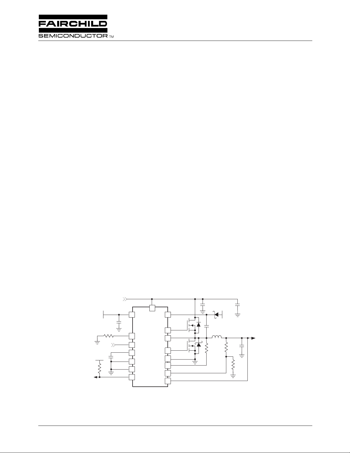
Typical Application
VIN (BATTERY)
+5
+5 9
Figure 1. 1.8V Output Regulator (see Table 2, page 12 for BOM)
= 2 to 24V
C4
R5
C3
R4
PGOOD
VC
ILIM
EN
SS1
FPWM
AGND
VI
N
C
11
4
3
7
16
8
2
1
FAN5234
BOOT
Q1A
H
DRV
14
SW
13
Q1B
L
DRV
10
PGND
IS
NS
12
SEN
V
6
VOUT
5
C1
C5
R3
L1
D1
C2
+515
1.8V@3.5A
R1
C6
R2
REV. 1.0.8 1/10/03

FAN5234 PRODUCT SPECIFICATION
Pin Configurations
VIN
PGOOD
ILIM
VOUT
VSEN
AGND
1
2
EN
3
4
FAN5234
5
6
SS
7
8
QSOP-16 or TSSOP-16
FPWM
16
BOOT
15
HDRV
14
SW
13
ISNS
12
VCC
11
LDRV
10
PGND
9
θJA = 112°C/W
Pin Definitions
Pin
Number Pin Name Pin Function Description
1 VIN
2 PGOOD Power Good Flag. An open-drain output that will pull LOW when VSEN is outside of a
3EN ENABLE . Enables operation when pulled to logic high. Toggling EN will also reset the
4 ILIM
5 VOUT
6 VSEN
7SS Soft Start. A capacitor from this pin to GND programs the slew rate of the converter
8 AGND
9 PGND
10 LDRV
11 VCC
12 ISNS
13 SW
14 HDRV
15 BOOT
16 FPWM Forced PWM mode. When logic HIGH, inhibits the regulator from entering hysteretic
Input Voltage. Connect to main input power source (battery). Also used to program
operating frequency for low input voltage operation. See Table 1.
±10% range of the 0.9V reference.
regulator after a latched fault condition. This is a CMOS inputs whose state is
indeterminate if left open.
Current Limit. A resistor from this pin to GND sets the current limit.
Output Voltage. Connect to output voltage. Used for regulation to ensure a smooth
transitions during mode changes. When VOUT is expected to exceed VCC, tie this pin to
VCC.
Output Voltage Sense. The feedback from the output. Used for regulation as well as
PGOOD, under-voltage, and over-voltage protection and monitoring.
during initialization. During initialization, this pin is charged with a 5 µ A current source.
Analog Ground. This is the signal ground reference for the IC. All voltage levels are
measured with respect to this pin.
Power Ground. The return for the low-side MOSFET driver. Connect to source of low-
side MOSFET.
Low-Side Drive. The low-side (lower) MOSFET driver output. Connect to gate of low-side
MOSFET.
VCC. This pin powers the chip as well as the LDRV buffers. The IC starts to operate when
voltage on this pin exceeds 4.6V (UVLO rising) and shuts down when it drops below 4.3V
(UVLO falling).
Current Sense input. Monitors the voltage drop across the lower MOSFET or external
sense resistor for current feedback.
Switching node. Return for the high-side MOSFET driver and a current sense input.
Connect to source of high-side MOSFET and low-side MOSFET drain.
High-Side Drive. High-side (upper) MOSFET driver output. Connect to gate of high-side
MOSFET.
BOOT. Positive supply for the upper MOSFET driver. Connect as shown in Figure 2.
mode.
REV. 1.0.8 1/10/03
2

) –
FAN5234 PRODUCT SPECIFICATION
Absolute Maximum Ratings
Absolute maximum ratings are the values beyond which the device may be damaged or have its useful life
impaired. Functional operation under these conditions is not implied.
Parameter Min. Typ. Max. Units
VCC Supply Voltage: 6.5 V
VIN 27 V
BOOT, SW, ISNS, HDRV 33 V
BOOT to SW 6.5 V
All Other Pins –0.3 VCC+0.3 V
Junction Temperature (T
Storage Temperature –65 150 °C
Lead Soldering Temperature, 10 seconds 300 °C
) –10 150 °C
J
Recommended Operating Conditions
Parameter Conditions Min. Typ. Max. Units
Supply Voltage VCC
Supply Voltage VIN
Ambient Temperature (T
A
4.75 5 5.25 V
524V
10 85 °C
REV. 1.0.8 1/10/03
3
PRODUCT SPECIFICATION FAN5234
µ
µ
µ
µ
µ
Ω
Ω
Ω
Ω
µ
Electrical Specifications
Parameter Conditions Min. Typ. Max. Units
Power Supplies
VCC Current LDRV, HDRV Open, VSEN forced
VIN Current - Sinking VIN pin = input voltage source 10 20 30
VIN Current - Sourcing VIN pin = GND 7 15 20
VIN Current - Shut-down 1
UVLO Threshold Rising VCC 4.3 4.55 4.75 V
Oscillator
Frequency VIN > 5V 255 300 345 KHz
Ramp Amplitude, pk–pk VIN = 16V 2 V
Ramp Amplitude, pk–pk VIN < 5V 1.25 V
Ramp Offset 0.5 V
Ramp / VIN Gain VIN >
Ramp / VIN Gain 1V < VIN < 3V 250 mV/V
Reference and Soft Start
Internal Reference Voltage 0.891 0.9 0.909 V
Soft Start current (I
Soft Start Complete Threshold 1.5 V
PWM Converter
Load Regulation I
VSEN Bias Current 50 80 120 nA
VOUT pin input impedance 40 55 65 K Ω
Under-voltage Shutdown as % of set point. 2 µ S noise filter 70 75 80 %
I
Over-Current threshold R
SNS
Over-voltage threshold as % of set point. 2 µ S noise filter 113 120 %
Output Driver
HDRV Output Resistance Sourcing 8 15
LDRV Output Resistance Sourcing 8 15
PGOOD (Power Good Output) and Control pins
Lower Threshold as % of set point, 2 µ S noise filter 86 92 %
Upper Threshold as % of set point, 2 µ S noise filter 110 115 %
PGOOD Output Low I
Leakage Current V
Soft Start Voltage when PGOOD
Enabled
EN, FPWM Inputs
Input High 2 V
Input Low 0.8 V
) at start-up 5
SS
Recommended operating conditions, unless otherwise noted.
850 1300 µ A
above regulation point
Shut-down (EN=0) 5 15
Falling 4.1 4.27 4.5 V
Hysteresis 0.1 0.5 V
VIN = 0V 510 600 690 KHz
3V 125 mV/V
from 0 to 3A, VIN from 2 to 24V -1 +1 %
OUT
= 68.5K Ω . See Figure 4 115 144 172 µA
ILIM
Sinking 3.2 4
Sinking 1.5 2.4
= 4mA 0.5 V
PGOOD
= 5V 1
PULLUP
1.5 V
A
A
A
A
A
A
4
REV. 1.0.8 1/10/03
FAN5234 PRODUCT SPECIFICATION
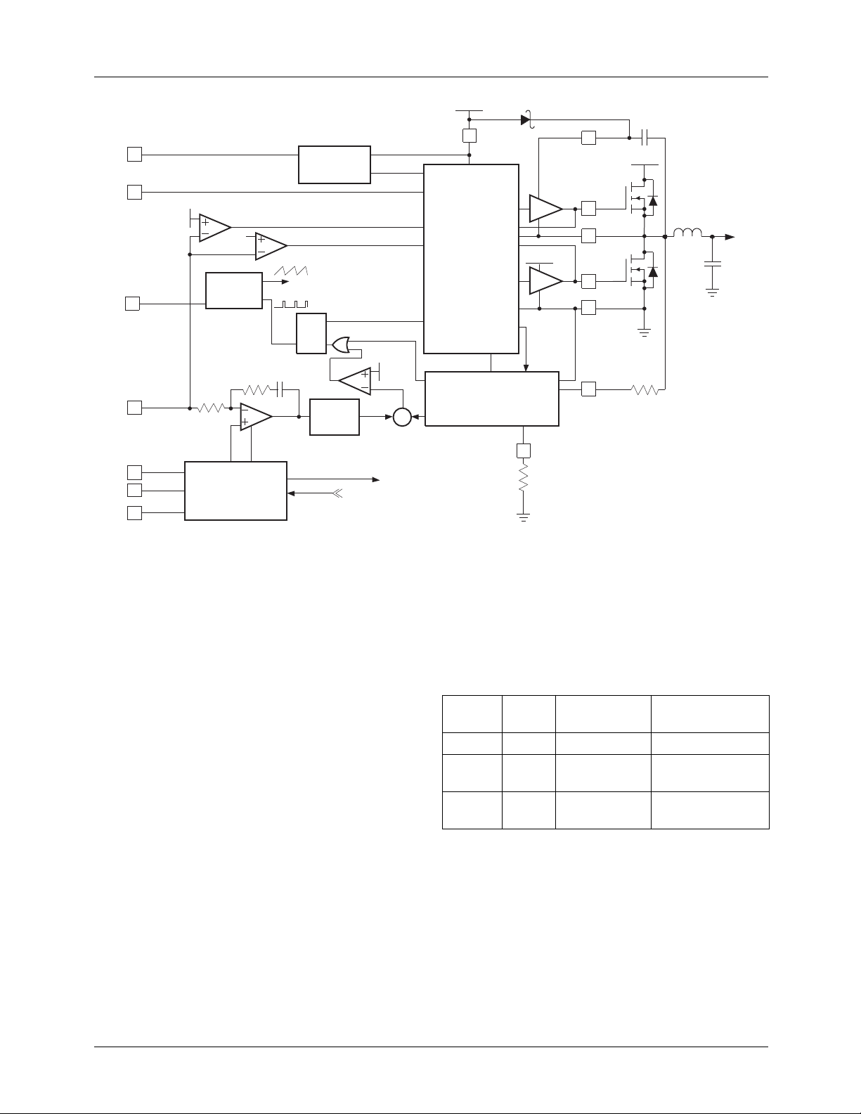
5V
EN
FPWM
VIN
VSEN
VDD
POR/UVLO
FPWM
HYST
SS
OVP
OSC
CL
RAMP
K
Q
SR
PWM
EA
DUTY
CYCLE
CLAMP
RAMP
HYST
ADAPTIVE
GATE
CONTROL LOGIC
PWM
PWM /HYST
ILIM det.
CURRENT PROCESSING
I
Σ
OUT
VDD
S/H
MODE
BOOT
HDRV
SW
LDRV
PGND
ISNS
Q1
Q2
R
VIN
SENSE
C
BOOT
VOUT
L
OUT
C
OUT
SS
P
GOOD
REF2
Reference and
Soft Start
VREF
PWM/HYS
T
Figure 2. IC Block Diagram
Circuit Description
Overview
The FAN5234 is a PWM controller intended for low voltage
power applications in modern notebook, desktop, and
sub-notebook PCs. The output voltage of the controller can
be set in the range of 0.9V to 5.5V by an external resistor
divider.
The synchronous buck converter can operate from either an
unregulated DC source (such as a notebook battery) with
voltage ranging from 2V to 24V, or from a regulated system
rail. In either mode of operation the IC is biased from a +5V
source. The PWM modulator uses an average current mode
control with input voltage feed-forward for simplified feedback loop compensation and improved line regulation. The
controller includes integrated feedback loop compensation
that dramatically reduces the number of external components.
Depending on the load level, the converter can operate either
in fixed frequency PWM mode or in a hysteretic mode.
Switch-over from PWM to hysteretic mode improves the
converters' efficiency at light loads and prolongs battery run
time. In hysteretic mode, a comparator is synchronized to the
main clock that allows seamless transition between the operational modes and reduced channel-to-channel interaction.
ILIM
R
ILIM
The hysteretic mode of operation can be inhibited independently using the FPWM pin if variable frequency operation is
not desired.
Oscillator
Table 1. Converter Operating modes
Mode
F
SW
(Khz)
Converter
Power VIN Pin
Battery 300 2 to 24V Battery (>5V)
Fixed
300 < 5.5V Fixed 100K Ω to GND
300
Fixed
600 < 5.5V Fixed GND
600
When VIN is from the battery, the oscillator's ramp amplitude is proportional to VIN, providing voltage feed-forward
control for improved loop response. When in either of the
Fixed modes, oscillator's ramp amplitude is fixed. The operating frequency is then determined according to the connection on the VIN pin (Table 1).
Initialization and Soft Start
Assuming EN is high, FAN5234 is initialized when VCC
exceeds the rising UVLO threshold. Should VCC drop below
the UVLO threshold, an internal Power-On Reset function
disables the chip.
REV. 1.0.8 1/10/03
5
 Loading...