

Fairchild Semiconductor FAN5231 Datasheet
www.fairchildsemi.com
FAN5231
Precision Dual PWM Controller And Linear
Regulator for Notebook CPUs
Features
• Provides 3 Regulated Voltages
– Microprocessor core (SpeedStep™-enabled)
– Microprocessor I/O
– Microprocessor Clock Generator
• High Efficiency Over Wide Load Range
• Not Dissipative Current-Sense Scheme
– Uses MOSFET’s R
– Optional Current-Sense Resistor for Precision
Overcurrent
• Adaptive Dead Time Drivers for N-Channel MOSFETs
• Operates from +5V, +3.3V and Battery (5.6-24V) Inputs
• Precision Core Voltage Control:
– Remote “Kelvin” Sensing
– Summing Current-Mode Control
– On-Chip Mode-Compensated “Droop” for Optimum
Transient Response and Lower Processor Power
Dissipation
DS(ON)
• TTL-Compatible 5-Bit Digital Output Voltage Selection
– Wide Range - 0.925VDC to 1.3VDC in 25mV Steps,
and from 1.3VDC to 2.0VDC in 50mV Steps
– Programmable “On-the-Fly” VID code change with
customer programmable slew rate and 100ms settling
time
• Power-Good Output Voltage Monitor
• No negative Core and I/O voltage on turn-off
• Over-Voltage, Under-Voltage and Over-Current Fault
Monitors
• 300kHz Fixed Switching Frequency
• Thermal Shut-Down
Applications
• Converters for Mobile Dual-Mode CPUs
• Web Tablets
• Internet Appliances
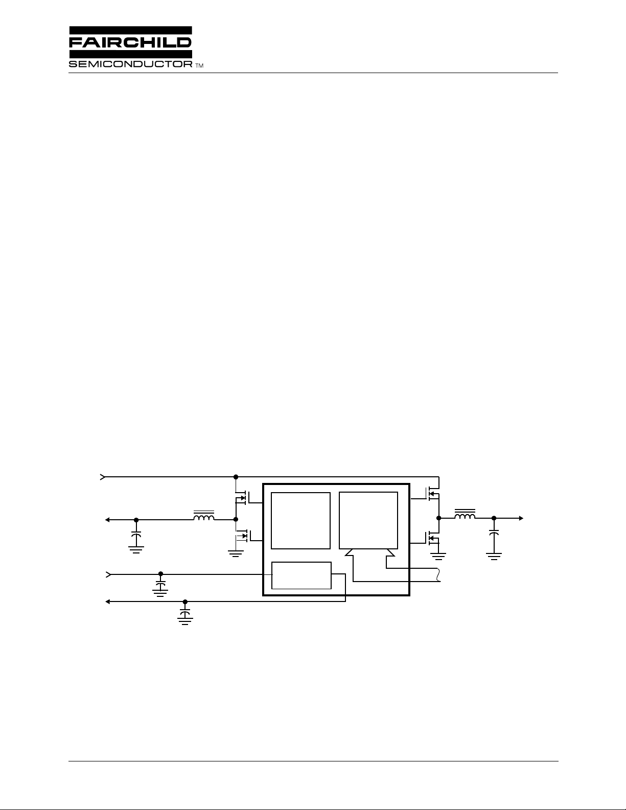
+V
IN
V
OUT2
I/
O
+V
IN
3.3V
V
OUT3
CPU CLK
PWM2
CONTROLLER
LI NEAR
REGULATO
Figure 1. Simplified Power System Diagram
R
PWM1
CONTRO
VI D CODE
LLER
FAN5231
V
OUT1
CORE
REV. 1.1.1 8/15/01
2
FAN5231
Description
The FAN5231 is a highly integrated power controller, which
provides a complete power management solution for mobile
CPUs. The IC integrates two PWM controllers and a linear
regulator as well as monitoring and protection circuitry into
a single 28-lead plastic SSOP package. The two PWM
controllers regulate the microprocessor core and I/O voltages
with synchronous-rectified buck converters, while the linear
regulator powers the CPU clock.
The FAN5231 includes 5-bit digital-to-analog converter
(DAC) that adjusts the core PWM output voltage from
0.925VDC to 2.0VDC and conforms to the Intel Mobile
VID specification. The DAC setting may be changed during
operation to accommodate Dual-Mode processors. Special
measures are taken to provide such a transition with controlled rate in a specified 100 µs. A precision reference,
remote sensing, and a proprietary architecture with integrated processor mode-compensated "droop" provide excellent static and dynamic core voltage regulation. The second
PWM controller has a fixed 1.5V output voltage and powers
the I/O circuitry. Both PWM controllers have integrated
feedback-loop compensation that dramatically reduces the
number of external components. At nominal loads PWM
controllers operate at fixed frequency 300kHz. At light loads
when the filter inductor current becomes discontinuous,
controllers operate in a hysteretic mode. The out-of-phase
operation of two PWM controllers reduces input current
ripple in both modes of operation. The linear regulator uses
an internal pass device to provide 2.5V for the CPU clock
generator.
The FAN5231 monitors all the output voltages. A single
Power-Good signal is issued when soft start is completed
and all outputs are within ±10% of their respective set points.
A built-in over-voltage protection for the core and I/O outputs forces the lower MOSFETs on to prevent output voltages from going above 115% of their settings. Under-voltage
protection latches the chip off when any of the three outputs
drops below 75% of the set value. The PWM controller's
overcurrent circuitry monitors the output current by sensing
the voltage drop across the lower MOSFETs. If precision
overcurrent protection is required, an external current-sense
resistor may be used.
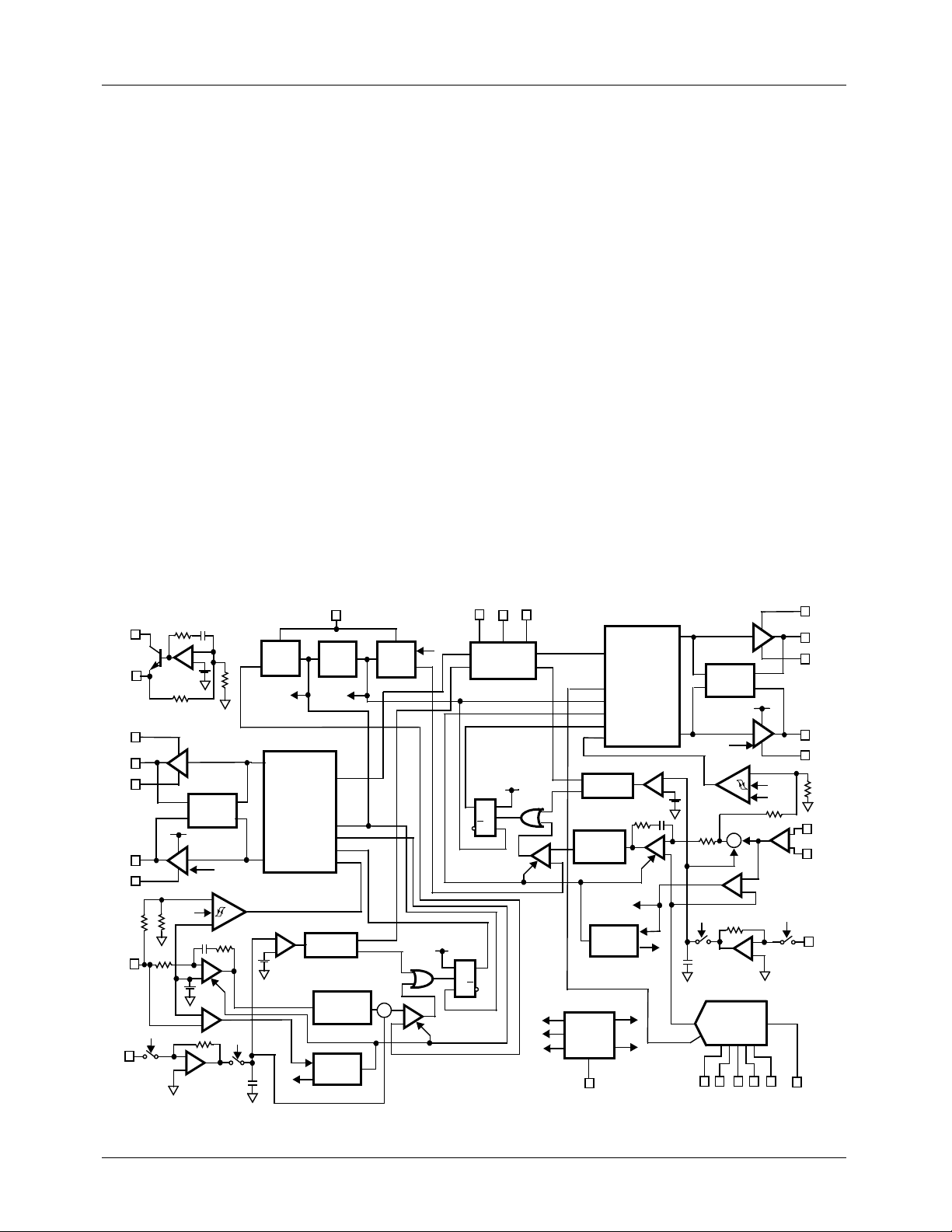
Block Diagram
LI NEAR REGULATOR
V3IN
-
VOUT 3
BOOT2
UGATE2
PHASE2
LGATE2
PGND2
VSEN2
MODE
CONTROL
COMP 2
LGATE2
ISEN2
0.9V
VCC
CLK2
R1=20k
+
+
-
HGDR2
GATE
CONTROL
LGDR2
OVP2
HYST COMP2
+
+
-
0.9V
+
-
+
-
+
EA2
LGATE2
RAM P 2
HI
GATE LOGI C 2
LO
OC COMP2
-
2.8V
+
-
VBATT
CLK
CLK 2 CLK1
FLOGO N
SHUTOFF
DEADT
PWM/HYS T
PWM ON
HYST ON
OC LOGI C2
+
DYNAMI C
DUTY CYCLE
CLAMP
MODE
CONTROL
PHASE1
LOGI C 1
RAMP 1
∑
EN
FFBK 1
PWM
LAT CH 1
PWM
VCC
LATCH 2
Q
D
R
Q
<
+
VCC
POWER-ON
RESET (POR)
VCC
Q
D
R
Q
<
GND
+
OC LOGI C1
DYNAM IC
DUTY CYCLE
CLAMP
MODE
CONTROL
LOGI C 1
OUTPUT
VOLTA GE
MONIT OR
PGOOD
FLOGO N
SHUTOFF
GATE LOGI C 1
FCCM
DEADT
PWM/HYS T
PWM ON
HYST ON
OC COMP1
EA1
FFBK 1
PHASE1
OVP1
OVP2
+
+
FCCM
+
-
LGATE1
BOOT1
UGATE1
PHASE1
LGATE1
PGND1
VSEN1
VRET1
ISEN1
+
-
CONTROL
HYST COMP1
LGATE1
REFERENCE
SOFT START
VI D0
VI D1
HGDR1
GATE
VCC
LGDR1
OVP1
CLK 1
+
DAC OUT
PRE AMP
∑
FAST FEEDBACK COMP1
+
R1= 20k
+
TTL DAC
VI D4 SOFT
VI D2
VI D3
HI
LO
DACOUT
REV. 1.1.1 8/15/01
FAN5231
Pinout
VCC
LGATE2
PGN D2
BOOT2
UGATE2
PHASE2
ISEN2
VI D4
VI D3
VI D2
VI D1
VI D0
VSEN2
V3IN
VOUT 3
1
2
3
4
5
6
7
8
9
10
11
12
13
14
28
27
26
25
24
23
22
21
20
19
18
17
16
15
LGA
TE1
PGND1
BOOT1
UGATE1
PHASE1
ISEN1
PGOOD
EN
VI N
SOFT
VSEN1
VRET1
GND
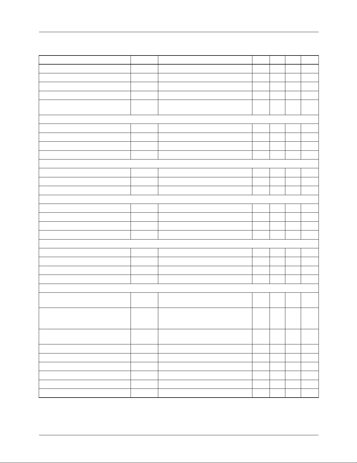
Absolute Maximum Ratings
Parameter Min. Max. Units
Supply Voltage, V
CC
Input Voltage, Vin + 29.0 V
V3in + 6.5 V
PHASE1,2 + 29.0 V
BOOT1,2 + 29.0 V
BOOT1,2 with respect to PHASE1,2 + 6.5 V
PGOOD, RT/FAULT, and GATE Voltage GND - 0.3 V
Core Output or I/O Voltage GND - 0.3 + 6.5 V
ESD Classification Class 2
CAUTION: Stresses above those listed in “Absolute Maximum Ratings” may cause permanent damage to the device. This is a
stress only rating and operation of the device at these or any other conditions above those indicated in the operational sections
of this specification is not implied.
+ 6.5 V
+ 0.3 V
CC
Recommended Operating Conditions
Parameter Min. Max. Units
Supply Voltage, V
CC
+5.0 ±5% V
Input Voltage, Vin +7.5 22.0 V
V3in +3.3 ±10% V
Ambient Temperature Range -20 85 °C
Junction Temperature Range -20 125 °C
Thermal Information
Parameter Min. Max. Units
Thermal Resistance (Typical, Note 1)
QSOP Package 55
QSOP Package (with 3 in
2
of copper) TBD
Maximum Junction Temperature (Plastic Package) 150 °C
Maximum Storage Temperature Range -65 150 °C
Maximum Lead Temperature (Soldering 10s)
(QSOP - Lead Tips Only)
Note
1. θ
is measured with the component mounted on an evaluation PC board in free air.
JA
θ
(°C/W)
JA
300 °C
REV. 1.1.1 8/15/01
3
FAN5231
4
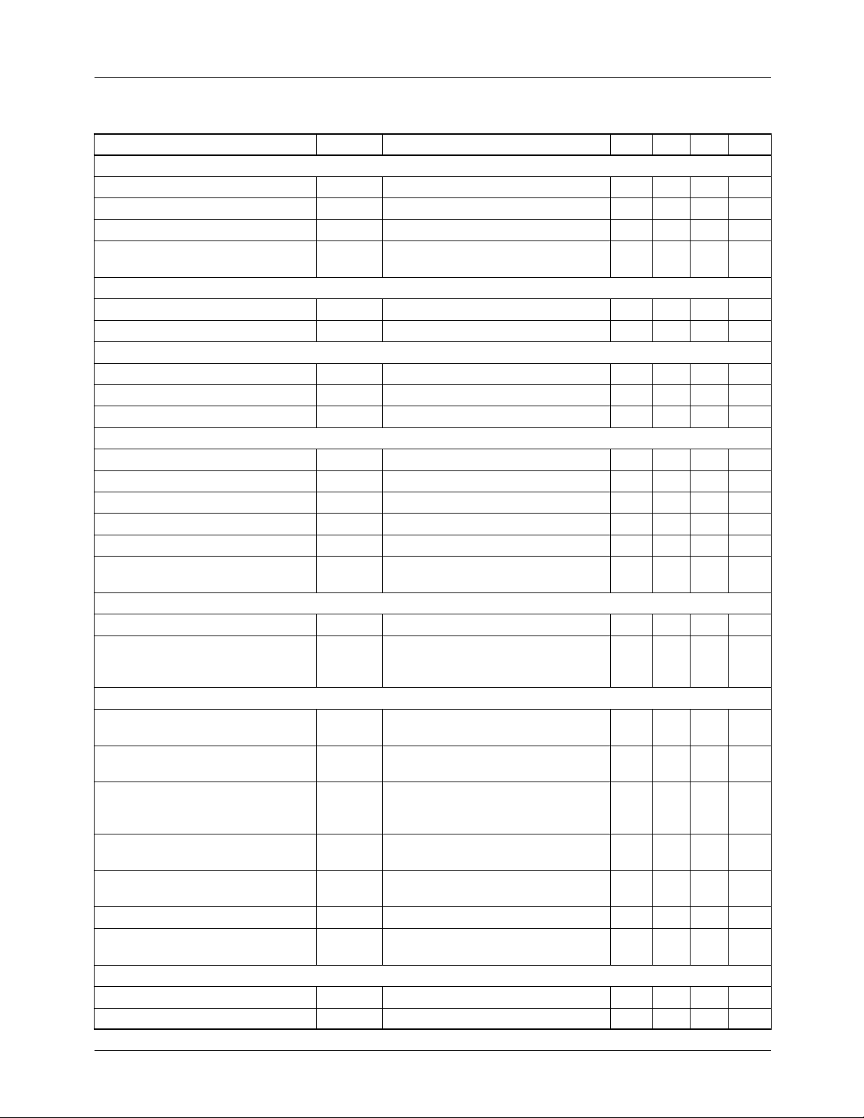
Electrical Specifications
(Recommended Operating Conditions, Unless Otherwise Noted. Refer to Figures 1, 2 and 3)
Parameter Symbol Test Condition Min. Typ. Max Units
VCC Supply
Nominal Supply Current I
Shut-down Supply Current I
Battery Pin Supply Current I
Battery Pin Leakage Current at
GATE1, GATE2 Open – 2 2.5 mA
CC
– 30 50 µA
CCS
– – 100 µA
VIN
I
VINSD
––5µA
Shut-Down
Power-On Reset
Rising VCC Threshold 4.3 4.5 4.6 V
Falling VCC Threshold 3.9 4.1 4.3 V
Oscillator
Free Running Frequency 255 300 345 kHz
Ramp Amplitude, pk-pk Vbat = 16V – 2 – V
Ramp Offset – 0.5 – V
Reference, DAC and Soft Start
VID0-VID4 Input Low Voltage – – 0.8 V
VID0-VID4 Input High Voltage 2.0 – – V
VID0-VID4 Pull-up Current to VCC – 1 – µA
DAC Voltage Accuracy Measured at pin 18 -1.0 – +1.0 %
Soft-Start Current During Start-Up I
Soft-Start Current During Mode
VSS = 0V…0.9V 18 27 36 µA
SS
I
SSM
VSS = 0.925V…2.0V 350 500 650 µA
Change
Enable
Enable Voltage Low V
Enable Voltage High V
ENLOW
ENHIGH
IC Inhibited – – 0.8 V
IC Enabled
2.0 – – V
Input has internal pull-up current
source 2µA typ
PWM 1 Converter
Output Voltage VOUT1 Defined by the current VID code
0.925 – 2.0 V
(Table 1)
Static Load Regulation 100mA < I
< 15.0A -2.0 – +2.0 %
VOUT1
Under-Voltage Shut-Down Level V
UV1
Percent of the voltage set by VID
70 75 80 %
code. Disabled during dynamic VID
code change.
Under-Voltage Shut Down Delay T
Over-Voltage V
DOC1
OVP1
Percent of the voltage set by VID
– 1.4 – µs
110 115 120 %
code.
Over-Voltage Shut Down Delay T
Over-Current Comparator
DOV1
I
OC1
– 2.4 – µs
100 135 170 µA
Threshold
PWM 2 Converter
Output Voltage VOUT2 1.5 V
Load Regulation 100mA < I
< 2.1A -2.0 – +2.0 %
VOUT3
REV. 1.1.1 8/15/01
FAN5231
Electrical Specifications
(Continued)
(Recommended Operating Conditions, Unless Otherwise Noted. Refer to Figures 1, 2 and 3)
Parameter Symbol Test Condition Min. Typ. Max Units
Under-Voltage Shut-Down Level V
Under-Voltage Shut Down Delay T
Over-Voltage Shut-Down V
Over-Voltage Shut Down Delay T
Over-Current Comparator
UV2
DOC2
OVP2
DOV2
I
OC2
1.05 – 1.20 V
– 1.4 – µs
1.65 – 1.80 V
– 2.4 – µs
100 135 170 µA
Threshold
Linear Regulator
Output Voltage VOUT3 2.5 V
Load Regulation 10mA < I
Under-Voltage Shut-Down Level V
Current Limit I
UV3
OC3
< 150mA -2.0 – 2.0 %
VOUT3
1.8 – 2.0 %
190 250 340 mA
PWM Controller Error Amplifiers
DC Gain By design – 86 – dB
Gain-Bandwidth Product GBWP By design – 2.7 – MHz
Slew Rate SR By design – 1 – V/µs
PWM 1 Controller Gate Drivers
Upper Drive Pull-Up Resistance R
Upper Drive Pull-Down Resistance R
Lower Drive Pull-Up Resistance R
Lower Drive Pull-Down Resistance R
1UGPUP
1UGPDN
1LGPUP
1LGPDN
–68 Ω
–35 Ω
–68 Ω
– 0.8 1.5 Ω
PWM 2 Controller Gate Drivers
Upper Drive Pull-Up Resistance R
Upper Drive Pull-Down Resistance R
Lower Drive Pull-Up Resistance R
Lower Drive Pull-Down Resistance R
2UGPUP
2UGPDN
2LGPUP
2LGPDN
–1220 Ω
–610 Ω
–1020 Ω
–610 Ω
Power Good
V
Upper Threshold Percent of the voltage defined by the
OUT1
108 – 114 %
VID code
V
Lower Threshold, Falling
OUT1
Edge
Percent of the voltage defined by the
VID code
85 – 92 %
V
Lower Threshold, Risisng
OUT1
Edge
V
Upper Threshold 1.60 – 1.75 V
OUT2
V
Lower Threshold 1.30 – 1.45 V
OUT2
V
Upper Threshold 2.65 – 2.85 V
OUT3
V
Lower Threshold 2.15 – 2.35 V
OUT3
PGOOD Voltage Low V
PGOOD Leakage Current I
REV. 1.1.1 8/15/01
PGOOD
PGlLKG
Percent of the voltage defined by the
VID code
I
V
= -1.6mA – – 0.4 V
PGOOD
= 5.0V – – 1.0 µA
PULLUP
87 – 94 %
5

FAN5231
6
Functional Pin Description
VID0, VID1, VID2, VID3, VID4 (Pins 11, 10, 9, 8
and 7 respectively)
VID0-VID4 are the input pins to the 5-bit DAC. The states of
these five pins program the internal voltage reference
(DACOUT). The level of DACOUT sets the core converter
output voltage (V
and OVP thresholds.
BOOT1, BOOT2 (Pins 25 and 3)
These pins provide power to the upper MOSFET drivers of
the core and I/O converters. Connect these pins to their
respective junctions of the bootstrap capacitors and the cathodes of the bootstrap diodes. The anodes of the bootstrap
diodes are connected to pin 28, VCC.
PHASE1, PHASE2 (Pins 23 and 5)
The PHASE nodes are the junction points of the upper MOSFET sources, output filter inductors, and lower MOSFET
drains. Connect the PHASE pins to the respective PWM converter’s upper MOSFET source.
ISEN1, ISEN2 (Pins 22 and 6)
These pins are used to monitor the voltage drop across the
lower MOSFETs for current feedback, output voltage droop
and over-current protection. For precise current detection
these inputs could be connected to optional current sense
resistors placed in series with sources of the lower MOSFETs. To set the gain of the current sense amplifier, a resistor
should be placed in series with each of these inputs.
UGATE1, UGATE2 (Pins 24 and 4)
These pins provide the gate drive for the upper MOSFETs.
LGATE1, LGATE 2 (Pin 27 and 1)
These pins provide the gate drive for the lower MOSFETs.
). It also sets the core PGOOD, UVP
OUT1
VOUT3 (Pin 14)
Output of the 2.5V linear regulator. Supplies current up to
150mA. The output current on this pin is internally limited to
250mA.
VSEN1, VRTN1 (Pins 17 and 16)
These pins are connected to the core converter’s output voltage to provide remote sensing. The PGOOD, UVP and OVP
comparators use this pins for protection.
SOFT (Pin 18)
Connect a capacitor from this pin to the ground. This capacitor (typically 0.1mF), along with an internal 25µA current
source, sets the soft-start interval of the converter. When
voltage on this pin exceeds 0.9V, the soft start is completed.
After the soft-start is completed, the pin function is changed.
The internal circuit regulates voltage on this pin to the value
commanded by VID code. The pin now has 500µA source/
sink capability that allows to set desired slew rate for upward
and downward VID code changes.
VIN (Pin 19)
VIN provides battery voltage to the oscillator for feed-forward rejection of input voltage variations.
EN (Pin 20)
This pin enables IC operation when left open or pulled-up to
VCC. Also, it unlatches the chip after fault when being
cycled.
PGOOD (Pin 21)
PGOOD is an open drain output used to indicate the status of
the PWM converters’ output voltages. This pin is pulled low
when the core output is not within ±10% of the DACOUT
reference voltage, or when any of the other outputs are not
within their respective under-voltage and over-voltage
thresholds.
PGND1, PGND2 (Pin 26 and 2)
These are the power ground connection for the core and I/O
converters, respectively. Tie each lower MOSFET source to
the corresponding pin.
VSEN2 (Pin 12)
This pin is connected to the I/O output and provides voltage
feedback to the I/O error amplifier. The PGOOD, UVP and
OVP comparators use this signal.
V3IN (Pin 13)
This pin provides input power for the 2.5V linear regulator.
The typical input voltage for that pin is 3.3V. Alternatively,
5.0V system rail can be used while efficiency will be proportionally lower.
The PGOOD output is pulled low for “01111” and ‘11111’
VID code. See Table 1.
GND (Pin 15)
Signal ground for the IC. All voltage levels are measured
with respect to this pin.
VCC (Pin 28)
Supplies all the power necessary to operate the chip. The IC
starts to operate when the voltage on this pin exceeds 4.5V
and shuts down when the voltage on this pin drops below
4.0V.
REV. 1.1.1 8/15/01
 Loading...