

Fairchild Semiconductor FAN5098 Datasheet
www.fairchildsemi.com
FAN5098
Two Phase Interleaved Synchronous Buck Converter
®
for AMD
Hammer™
Features
• Programmable output from 800mV to 1.550V in 25mV
steps using an integrated 5-bit DAC
• Two interleaved synchronous phases for maximum
performance
• 100nsec transient response time
• Built-in current sharing between phases
• Remote sense
• Programmable Active Droop
(Voltage Positioning)
• Programmable switching frequency from 100KHz to
1MHz per phase
• Adaptive delay gate switching
• Integrated high-current gate drivers
• Integrated Power Good, OV, UV, Enable/Soft Start
functions
• Drives N-channel MOSFETs
• Operation optimized for 12V operation
• High efficiency mode (E*) at light load
• Overcurrent protection using MOSFET sensing
• 24 pin TSSOP package
Applications
• VRM/VRD for 64-Bit Athlon™ and Opteron™ CPU’s
• VRM/VRD for Advanced CPU’s
• Programmable step-down power supply
Description
The FAN5098 is a synchronous two-phase DC-DC controller
IC which provides a highly accurate, programmable output
voltage for the AMD
leaved synchronous buck regulator phases with built-in current sharing operate 180° out of phase to provide the fast
transient response needed to satisfy high current applications
while minimizing external components.
The FAN5098 features Programmable Active Droop
transient response with minimum output capacitance. It has
integrated high-current gate drivers, with adaptive delay gate
switching, eliminating the need for external drive devices.
The FAN5098 uses a 5-bit D/A converter to program the output voltage from 800mV to 1.550V in 25mV steps with an
accuracy of 1%. The FAN5098 uses a high level of integration to deliver load currents in excess of 50A from a 12V
source with minimal external circuitry.
The FAN5098 also offers integrated functions including
Power Good, Output Enable/Soft Start, under-voltage lockout, over-voltage protection, and adjustable current limiting
with independent current sense on each phase. It is available
in a 24 pin TSSOP package.
®
Hammer™ processor. Two inter-
for
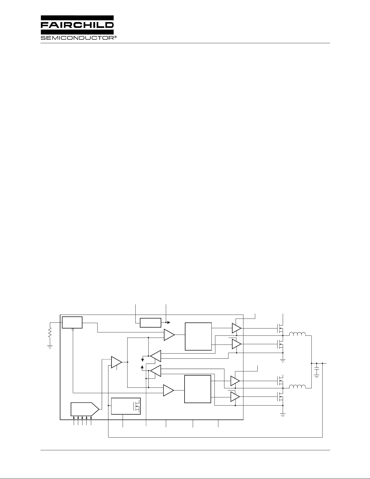
Block Diagram
23
OSC
R
T
-
+
GNDA
24
Power
Good
19
PWRGD
5-Bit
DAC
5
1234
VID2
VID1
VID3
VID4
VID0
Athlon™ and Hammer™ are registered trademarks of AMD
BYPASS
6
5V Reg
Current
Limit
DROOP/E*
®
. Programmable Active Droop is a trademark of Fairchild Semiconductor.
+12V
18
O
UVL
+
-
-
+
-
+
-
+
21
7
AGND
Digital
Control
Digital
Control
22
ENABLE/SS
+12V
+12V
20
ILIM
BOOT A
13
14
15
17
16
12
11
10
8
9
BOOT B
+12V
VO
+12V
REV. 1.0.7 2/18/03
FAN5098 PRODUCT SPECIFICATION
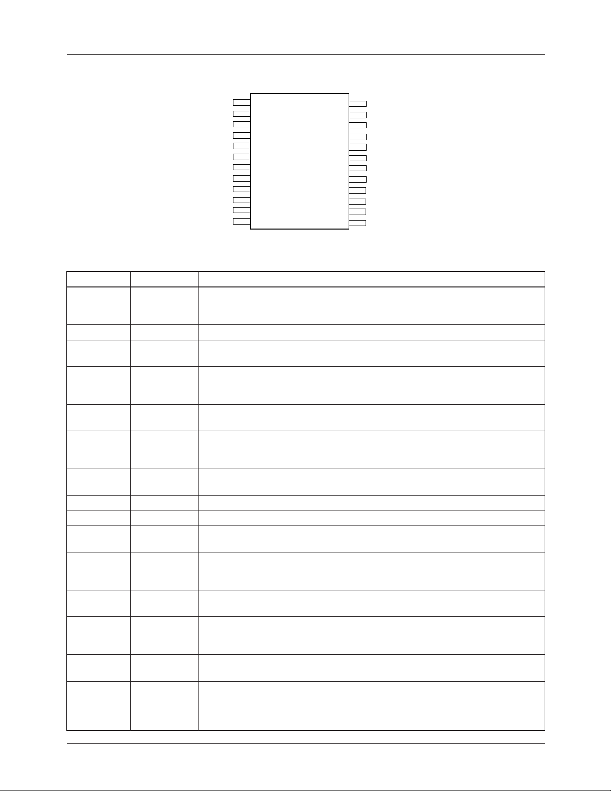
Pin Assignments
VID0
VID1
VID2
VID3
VID4
BYPASS
AGND
LDRVB
PGNDB
SWB
HDRVB
BOOTB
1
2
3
4
5
6
7
8
9
10
11
12
FAN5098
Pin Definitions
Pin Number Pin Name Pin Function Description
1-5 VID0-4
6 BYPASS
7 AGND
8 LDRVB
9 PGNDB
10 SWB
11 HDRVB
12 BOOTB
13 BOOTA
14 HDRVA
15 SWA
16 PGNDA
17 LDRVA
18 VCC
19 PWRGD
Voltage Identification Code Inputs. Open collector/TTL compatible inputs will
program the output voltage over the ranges specified in Table 1. Internally PulledUp.
5V Rail. Bypass this pin with a 0.1 µ F ceramic capacitor to AGND.
Analog Ground. Return path for low power analog circuitry. This pin should be
connected to a low impedance system ground plane to minimize ground loops.
Low Side FET Driver for B. Connect this pin to the gate of an N-channel
MOSFET for synchronous operation. The trace from this pin to the MOSFET gate
should optimally be <0.5 " .
Power Ground B. Return pin for high currents flowing in low-side MOSFET.
Connect directly to low-side MOSFET source.
High side driver source and low side driver drain switching node B. Gate
drive return for high side MOSFET, and negative input for low-side MOSFET
current sense.
High Side FET Driver B. Connect this pin to the gate of an N-channel MOSFET.
The trace from this pin to the MOSFET gate should optimally be <0.5 " .
Bootstrap B. Input supply for high-side MOSFET.
Bootstrap A. Input supply for high-side MOSFET.
High Side FET Driver A. Connect this pin to the gate of an N-channel MOSFET.
The trace from this pin to the MOSFET gate should optimally be <0.5 " .
High side driver source and low side driver drain switching node A. Gate
drive return for high side MOSFET, and negative input for low-side MOSFET
current sense.
Power Ground A. Return pin for high currents flowing in low-side MOSFET.
Connect directly to low-side MOSFET source.
Low Side FET Driver for A. Connect this pin to the gate of an N-channel
MOSFET for synchronous operation. The trace from this pin to the MOSFET gate
should optimally be <0.5 " .
VCC. Internal IC supply. Connect to system 12V supply, and decouple with a 10 Ω
resistor and 1 µ F ceramic capacitor.
Power Good Flag. An open collector output that will be logic LOW if the output
voltage is less than 350mV less than the nominal output voltage setpoint. Power
Good is prevented from going low until the output voltage is out of spec for
500µsec.
24
23
22
21
20
19
18
17
16
15
14
13
VFB
RT
ENABLE/SS
DROOP/E*
ILIM
PWRGD
VCC
LDRVA
PGNDA
SWA
HDRVA
BOOTA
2
REV. 1.0.7 2/18/03
°
° C
°
16 °
84 °
°
PRODUCT SPECIFICATION FAN5098
Pin Number Pin Name Pin Function Description
20 ILIM
21 DROOP/E*
Current Limit. A resistor from this pin to ground sets the over current trip level.
Droop Control/Energy Star Mode Control. A resistor from this pin to ground
sets the amount of droop by controlling the gain of the current sense amplifier.
When this pin is pulled high to BYPASS, the phase A drivers are turned off for
Energy-star operation.
22 ENABLE/SS Output Enable/Softstart. A logic LOW on this pin will disable the output. An
10µA internal current source allows for open collector control. This pin also
doubles as soft start.
23 RT
24 VFB
Frequency Set. A resistor from this pin to ground sets the switching frequency.
Voltage Feedback. Connect to the desired regulation point at the output of the
converter.
Absolute Maximum Ratings
(Absolute Maximum Ratings are the values beyond which the device
may be damaged or have it’s useful life impaired. Functional operation under these conditions is not implied.)
Parameter Min. Max. Unit
Supply Voltage VCC 15 V
Supply Voltages BOOT to PGND 24 V
BOOT to SW 24 V
Voltage Identification Code Inputs, VID0-VID4 6 V
VFB, ENABLE/SS, PWRGD, DROOP/E* 6 V
SWA, SWB to AGND (<1µs) -3 15 V
PGNDA, PGNDB to AGND -0.5 0.5 V
Gate Drive Current, peak pulse 3 A
Junction Temperature, T
J
-55 150
C
Storage Temperature -65 150
Thermal Ratings
Parameter Min. Typ. Max. Unit
Lead Soldering Temperature, 10 seconds 300
Power Dissipation, P
Thermal Resistance Junction-to-Case, Θ
D
JC
Thremal Resistance Junction-to-Ambient, Θ
JA
650 mW
C
C/W
C/W
Recommended Operating Conditions (See Figure 2)
Parameter Conditions Min. Max. Units
Output Driver Supply, BOOTA, B 16 22 V
Ambient Operating Temperature 0 70
Supply Voltage V
REV. 1.0.7 2/18/03
CC
10.8 13.2 V
C
3
•
•
•
∆
•
FAN5098 PRODUCT SPECIFICATION
Electrical Specifications
(V
= 12V, VID = [00100] = 1.450V, and T
CC
The • denotes specifications which apply over the full operating temperature range.
Parameter Conditions Min. Typ. Max. Units
Input Supply
UVLO Hysteresis 1.0 V
12V UVLO Rising Edge
12V Supply Current PWM Output Open 20 mA
Internal Voltage Regulator
BYPASS Voltage 4.75 5 5.25 V
BYPASS Capacitor 100 nF
VREF and DAC
Output Voltage See Table 1
Initial Voltage Setpoint
1
Output Temperature Drift T
Line Regulation V
2
Droop
Programmable Droop Range 0 1.25 m Ω
Response Time
Current Mismatch R
VID Inputs
Input LOW current, VID pins V
VID V
IH
VID V
IL
No CPU VID Latency VID = [11111] to PWM low 200 ns
Oscillator
Oscillator Frequency RT = 54.9k Ω
Oscillator Range RT = 137.5k Ω to 13.75 k Ω
Maximum Duty Cycle RT = 137.5k Ω
Minimum LDRV on-time RT = 13.75k Ω
Gate Drive
Gate Drive On-Resistance 1.0
Output Driver Rise & Fall Time See Figure 1, C
Enable/Soft Start
Soft Start Current 10 µA
Enable Threshold ON
Power Good
PWRGD Threshold Logic LOW, V
PWRGD Output Voltage I
PWRGD Delay High → Low 500 µsec
PWRGD Delay Low → High 5 20 ms
OVP and OTP
Output Overvoltage Detect • 2.1 2.3 V
Over Temperature Shutdown 130 140 150 °C
Over Temperature Hysteresis 40 °C
Notes:
1. As measured at the converter’s VFB sense point. For motherboard applications, the PCB layout should exhibit no more than
0.5m Ω trace resistance between the converter’s output capacitors and the CPU. Remote sensing should be used for optimal
performance. Nominal output is offset +25mV vs. VID table.
2. Using the VFB pin for remote sensing of the converter’s output at the load, the converter will be in compliance with AMD
specification of V
DAC
±50mV.
= +25°C using circuit in Figure 2, unless otherwise noted.)
A
8.5 9.6 10.4 V
0.800 1.550 V
I
= 0A, VID = [00100] 1.466 1.475 1.489 V
LOAD
= 0 to 70°C5mV
A
= 11.4V to 12.6V
CC
I
= 52A, R
LOAD
V
= 10mV 100 nsec
out
(A) = R
DS,on
I
= 52A Droop = 1m Ω
LOAD
= 0.4V -60 µA
VID
DROOP
DS,on
= 4.99k Ω
(B),
130 µV
23 mV
5%
2.0 V
0.8 V
440 500 560 kHz
200 2000 kHz
90 %
330 nsec
= 3000pF 20 nsec
L
1.0
OFF
– V
VID
PWRGD
= 4mA 0.4 V
sink
300 350 367 mV
0.4
V
Ω
•
®
4
REV. 1.0.7 2/18/03
PRODUCT SPECIFICATION FAN5098
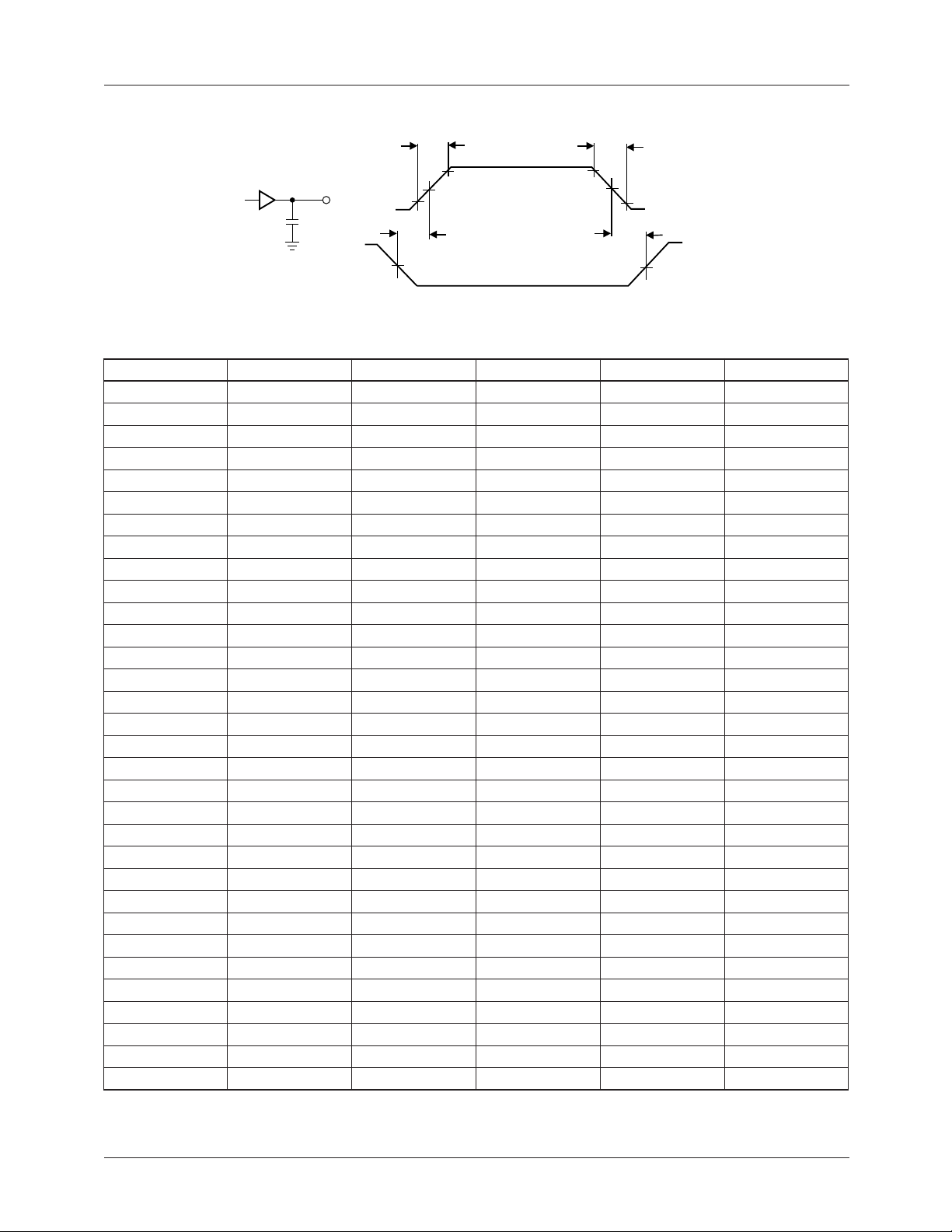
Gate Drive Test Circuit
3000pF
t
R
90%
t
DT
1.2V
2V
V
OUT
10%
90%
2.5V
t
10%
t
DT
2V
Figure 1. Output Drive Timing Diagram
Table 1. Output Voltage Programming Codes
VID4 VID3 VID2 VID1 VID0 V
11111OFF
111100.800V
111010.825V
111000.850V
110110.875V
110100.900V
110010.925V
110000.950V
101110.975V
101101.000V
101011.025V
101001.050V
100111.075V
100101.100V
100011.125V
100001.150V
011111.175V
011101.200V
011011.225V
011001.250V
010111.275V
010101.300V
010011.325V
010001.350V
001111.375V
001101.400V
001011.425V
001001.450V
000111.475V
000101.500V
000011.525V
000001.550V
HDRV
LDRV
OUT
to CPU
Note: Nominal output is typically offset +25mV from VID table.
REV. 1.0.7 2/18/03 5
FAN5098 PRODUCT SPECIFICATION
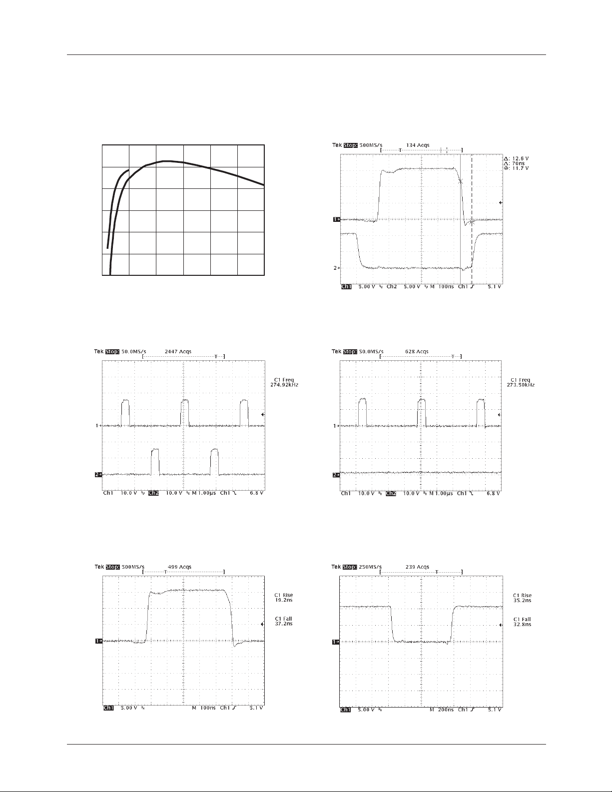
Typical Operating Characteristics
(VCC = 12V, VIN = 12V, V
= 1.450V and TA = +25°C using circuit in Figure 2, unless otherwise noted.)
OUT
EFFICIENCY VS. OUTPUT CURRENT
90
85
E* Mode
2 Phase Mode
80
75
70
EFFICIENCY (%)
65
60
010203040
50 60
LOAD CURRENT (A)
HIGH-SIDE GATE DRIVES, NORMAL OPERATION
CH1: HDRVB
CH2: HDRVA
10A Load
TRANSIENT RESPONSE, 20A to 0.25A
CH1: HDRVB
CH2: LDRVB
40A Load
HIGH-SIDE GATE DRIVES, E*-MODE
CH1: HDRVB
CH2: HDRVA
10A Load
ADAPTIVE GATE DELAY
HIGH-SIDE GATE DRIVES, RISE / FALL TIME
CH1: HDRVB
40A Load
LOW-SIDE GATE DRIVES, RISE / FALL TIME
CH1: LDRVB
40A Load
6 REV. 1.0.7 2/18/03
 Loading...