

Fairchild Semiconductor FAN5092 Datasheet
www.fairchildsemi.com
FAN5092
High Current System Voltage Buck Converter
Features
• Output from 1.1V to 5V
• Integrated high-current gate drivers
• T w o interlea v ed synchronous phases per IC for maximum
performance
• Up to 4 phase power system
• Built-in current sharing between phases and between ICs
• Frequency and phase synchronization between ICs
• Remote sense and Programmable Active Droop™
• High precision voltage reference
• High speed transient response
• Programmable frequency from 200KHz to 2MHz
• Adaptive delay gate switching
• Integrated Power Good, OV, UV, Enable/Soft Start
functions
• Drives N-channel MOSFETs
• Operation optimized for 12V
• High efficiency mode at light load
• Overcurrent protection using MOSFET sensing
• 28 pin TSSOP package
Applications
• Power supply for Logic
• Modular Power supply
Description
The FAN5092 is a synchronous multi-slice DC-DC
controller IC which provides a highly accurate,
programmable output voltage for all high-current
applications. Two interleaved synchronous buck regulator
phases with built-in current sharing operate 180 ° out of
phase to provide the fast transient response needed to satisfy
high current applications while minimizing external
components. F AN5092s can be paralleled while maintaining
both frequency and phase synchronization and ensuring
current sharing in a high-power system. The FAN5092
features remote voltage sensing, Programmable Active
Droop and advanced response for optimal converter
transient response with minimum output capacitance. It has
integrated high-current gate drivers with adaptive delay gate
switching, eliminating the need for external drive devices.
These make it possible to create power supplies running at a
switching frequency as high as 4MHz, for ultra-high density .
The output voltage can be set from 1.1V to 5V with an
accuracy of 0.5%. The FAN5092 uses a high level of
integration to deliver load currents in e xcess of 150A from a
12V source with minimal external circuitry. The FAN5092
also offers integrated functions including Power Good,
Output Enable/Soft Start, under-voltage lockout, overvoltage protection, and current limiting with independent
current sense on each slice. It is available in a 28-pin TSSOP
package.
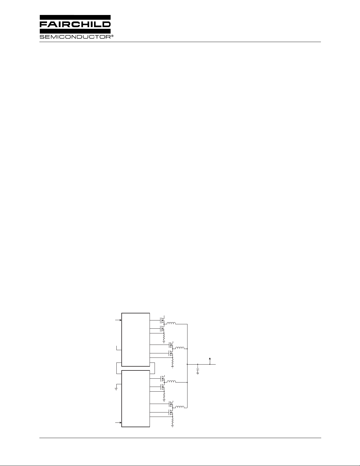
Block Diagram
VFB
FAN5092
+
PHASE
ISHR
CLK
ISHR
CLK
PHASE
FAN5092
VFB
Programmable Active Droop is a trademark of Fairchild Semiconductor.
+12V
+12V
+12V
+12V
+
VFB
3.3V @ 120A
REV. 1.0.7 6/20/02
FAN5092 PRODUCT SPECIFICATION
Pin Assignments
VID0
VID1
VID2
VID3
VID4
CLK
BYPASS
AGND
LDRVB
GNDB
ISNSB
SWB
HDRVB
BOOTB
1
2
3
4
5
6
7
8
9
10
11
12
13
14
FAN5092
28
27
26
25
24
23
22
21
20
19
18
17
16
15
VFB
RT
ENABLE/SS
DROOP/E*
ISHR
PHASE
PWRGD
VCC
LDRVA
GNDA
ISNSA
SWA
HDRVA
BOOTA
Pin Definitions
Pin Number Pin Name Pin Function Description
1-5 VID0-4
6 CLK
7 BYPASS
8 AGND
9 LDRVB
10 GNDB
11 ISNSB
12 SWB
13 HDRVB
14 BOOTB
15 BOOTA
16 HDRVA
17 SWA
18 ISNSA
Voltage Identification Code Inputs. These open collector/TTL compatible
inputs will program the output voltage over the ranges specified in Table 1.
Clock. When PHASE is high, this pin puts out a clock signal synchronized
180 ° out of phase with the internal master clock. When PHASE is low, this pin
is an input for a synchronizing clock signal.
5V Rail. Bypass this pin with a 0.1 µ F ceramic capacitor to AGND.
Analog Ground. Return path for low power analog circuitry. This pin should
be connected to a low impedance system ground plane to minimize ground
loops.
Low Side FET Driver for B. Connect this pin to the gate of an N-channel
MOSFET for synchronous operation. The trace from this pin to the MOSFET
gate should be <0.5”.
Ground B. Ground-side current sense pin. Connect directly to low-side
MOSFET source, or to sense resistor ground.
Current Sense B. Sensor side of current sense. Attach to low-side MOSFET
drain, or to source side of sense resistor.
High side driver source and low side driver drain switching node B. Gate
drive return for high side MOSFET, and negative input for low-side MOSFET
current sense.
High Side FET Driver B. Connect this pin to the gate of an N-channel
MOSFET. The trace from this pin to the MOSFET gate should be <0.5”.
Bootstrap B. Input supply for high-side MOSFET.
Bootstrap A. Input supply for high-side MOSFET.
High Side FET Driver A. Connect this pin to the gate of an N-channel
MOSFET. The trace from this pin to the MOSFET gate should be <0.5”.
High side driver source and low side driver drain switching node A. Gate
drive return for high side MOSFET, and negative input for low-side MOSFET
current sense.
Current Sense A. Sensor side of current sense. Attach to low-side MOSFET
drain, or to source side of sense resistor.
2
REV. 1.0.7 6/20/02
°
°
°
16 °
PRODUCT SPECIFICATION FAN5092
Pin Definitions
Pin Number Pin Name Pin Function Description
19 GNDA
20 LDRVA
21 VCC
22 PWRGD
23 PHASE
24 ISHR
25 DROOP/E*
26 ENABLE/SS
27 RT
28 VFB
(continued)
Ground A. Ground-side current sense pin. Connect directly to low-side
MOSFET source, or to sense resistor ground.
Low Side FET Driver for A. Connect this pin to the gate of an N-channel
MOSFET for synchronous operation. The trace from this pin to the MOSFET
gate should be <0.5”.
VCC. Internal IC supply. Connect to system 12V supply, and decouple with a
0.1 µ F ceramic capacitor.
Power Good Flag. An open collector output that will be logic LOW if the
output voltage is not within +11/–12% of the nominal output voltage setpoint.
Phase Control. Connecting this pin to bypass causes a synchronized clock
signal to appear on CLK. Connecting this pin to ground allows the CLK pin to
accept a clock signal for synchronization.
Current Share. Connecting this pin to the ISHR pin of another FAN5092
enables current sharing.
Droop Control/E*-mode Control. A resistor from this pin to ground sets the
amount of droop by controlling the gain of the current sense amplifier.
Connecting this pin to bypass turns off Phase A.
Output Enable. A logic LOW on this pin will disable the output. An internal
current source allows for open collector control. This pin also doubles as soft
start.
Frequency Set. A resistor from this pin to ground sets the switching
frequency. See Apps section.
Voltage Feedback. Connect to the desired regulation point at the output of
the converter.
Absolute Maximum Ratings
Parameter Min. Typ. Max. Units
Supply Voltage VCC 15 V
Supply Voltages BOOTA, BOOTB 22 V
Voltage Identification Code Inputs, VID0-VID4 6 V
VFB, ENABLE/SS, PHASE, CLK 6 V
PWRGD 15 V
SW, ISNS -3 15 V
PGNDA, PGNDB to AGND -0.5 0.5 V
Gate Drive Current, peak pulse 3 A
Junction Temperature, T
Storage Temperature -65 150
Lead Soldering Temperature, 10 seconds 300
Thermal Resistance Junction-to-case, Θ
J
JC
-55 150
C
C
C
C/W
REV. 1.0.7 6/20/02
3
°
•
•
µ
•
•
∆
Ω
FAN5092 PRODUCT SPECIFICATION
Recommended Operating Conditions
Parameter Conditions Min. Typ. Max. Units
Output Driver Supply, Boot 16 17 V
V
CC
10.8 12 13.2 V
Input Logic HIGH 2.0 V
Input Logic LOW 0.8 V
Ambient Operating Temperature 0 70
Electrical Specifications
(V
= 12V, V
CC
The • denotes specifications which apply over the full operating temperature range.
Output Voltage See Table I
Output Current 60 A
Internal Reference Voltage 1.4675 1.4750 1.4825 V
Initial Voltage Setpoint I
Output Temperature Drift T
Line Regulation V
Droop I
Programmable Droop Range R
Total Output Variation, Steady
1
State
Total Output Variation,
Transient
Response Time
Gate Drive On-Resistance 1.0
Upper Drive Low Voltage V
Upper Drive High Voltage V
Lower Drive Low Voltage I
Lower Drive High Voltage V
Output Driver Rise & Fall Time See Figure 2 20 nsec
Current Mismatch R
Output Overvoltage Detect
Efficiency I
Oscillator Frequency RT = 41.2K Ω•
Oscillator Range RT = 125K Ω to 12.5K Ω
Maximum Duty Cycle RT = 125K Ω
Minimum LDRV on-time RT=12.5K Ω
Input Low Current, VID pins V
Soft Start Current 10
Enable Threshold ON
BYPASS Voltage 4.75 5 5.25 V
= 1.500V, and T
OUT
= +25°C using circuit in Figure 1, unless otherwise noted.)
A
Parameter Conditions Min. Typ. Max. Units
1.100 1.850 V
= 5A 1.460 1.475 1.490 V
LOAD
= 0 to 70 ° C-5mV
A
= 11.4V to 12.6V
IN
= 0.8A to I
LOAD
= TBD to TBD -10 0 %V
DROOP
I
= 0.8A to I
LOAD
I
= 0.8A to I
2
LOAD
V
= 10mV 100 nsec
OUT
– V
HDRV
– V
BOOT
= 10µA 0.2 V
sink
– V
CC
LDRV
(A) = R
DS,on
at I
SW
HDRV
at I
max
max
max
= 10µA 0.2 V
sink
at I
source
DS,on
= 10µA 0.5 V
source
= 10µA 0.5 V
(B) 5 %
-90 -100 -110 mV
1.430 1.570 V
1.430 1.570 V
+130
2.1 2.3 V
= I
LOAD
I
LOAD
,
max
= 2A, E*-mode enabled
85
70
450 600 750 KHz
200 2000 KHz
90 %
330 nsec
= 0.4V 50 µA
VID
1.0 V
OFF 0.4
•
µ
C
V
OUT
%
A
4
REV. 1.0.7 6/20/02
PRODUCT SPECIFICATION FAN5092
Electrical Specifications (continued)
(VCC = 12V, V
The • denotes specifications which apply over the full operating temperature range.
BYPASS Capacitor 220 1000 nF
PWRGD Threshold Logic LOW, minimum
PWRGD Hysteresis 20 mV
PWRGD Output Voltage I
PWRGD Delay High → Low 500 µsec
12V UVLO • 8.5 9.5 10.5 V
UVLO Hysteresis 1.0 V
12V Supply Current HDRV and LDRV open 20 mA
Over Temperature Shutdown 150 °C
Over Temperature Hysteresis 25 °C
Notes:
1. Steady State Voltage Regulation includes Initial Voltage Setpoint, Output Ripple and Output Temperature Drift and is
measured at the converter’s VFB sense point.
2. As measured at the converter’s VFB sense point. Remote sensing should be used for optimal performance.
= 1.500V, and TA = +25°C using circuit in Figure 1, unless otherwise noted.)
OUT
Parameter Conditions Min. Typ. Max. Units
••81
Logic LOW, maximum
= 4mA 0.4 V
sink
108
85
111
89
115
%V
out
REV. 1.0.7 6/20/02
5

FAN5092 PRODUCT SPECIFICATION
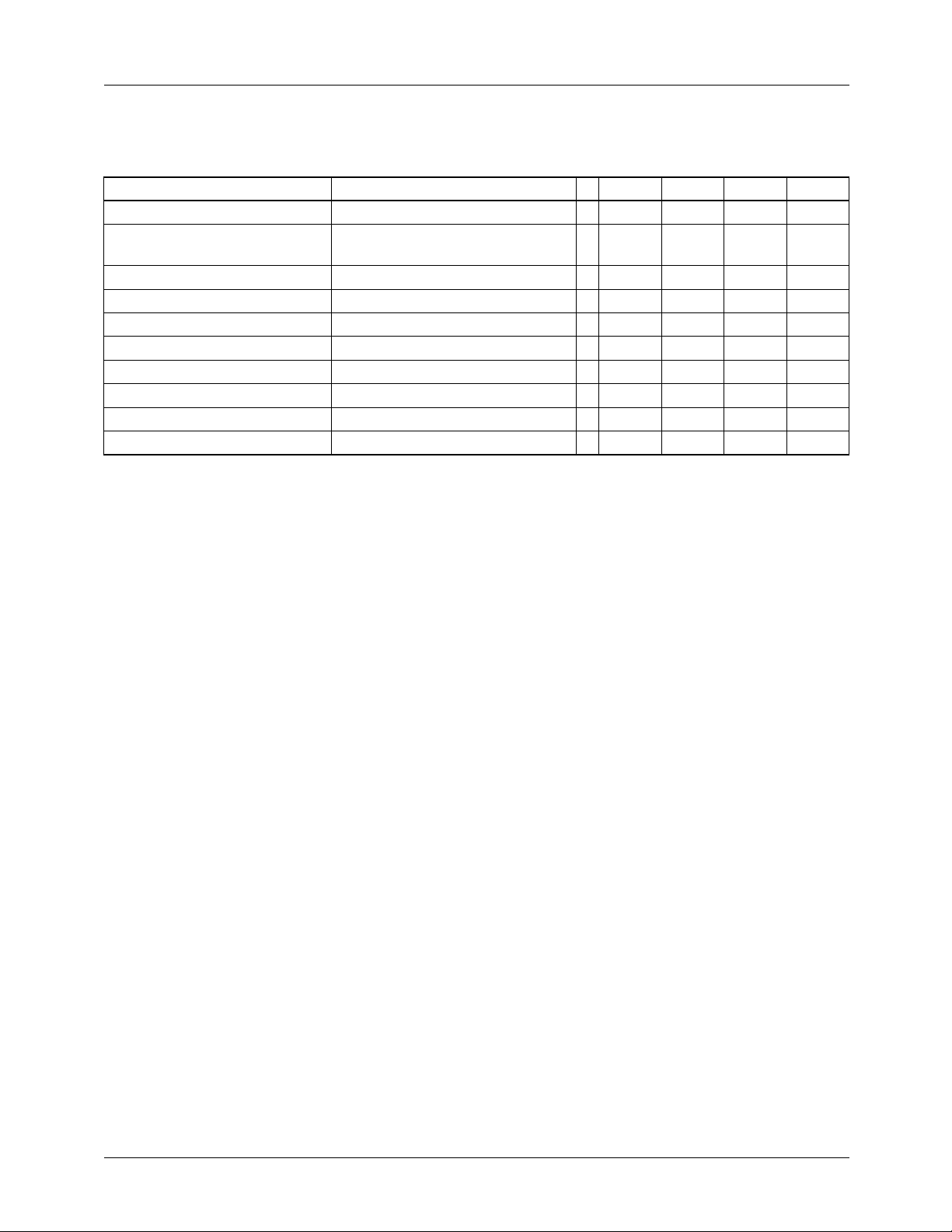
Table 1. Output Voltage Programming Codes
VID4 VID3 VID2 VID1 VID0 V
11111OFF
111101.100V
111011.125V
111001.150V
110111.175V
110101.200V
110011.225V
110001.250V
101111.275V
101101.300V
101011.325V
101001.350V
100111.375V
100101.400V
100011.425V
100001.450V
011111.475V
011101.500V
011011.525V
011001.550V
010111.575V
010101.600V
010011.625V
010001.650V
001111.675V
001101.700V
001011.725V
001001.750V
000111.775V
000101.800V
000011.825V
000001.850V
OUT
to CPU
Note:
1. 0 = VID pin is tied to GND.
1 = VID pin is pulled up to 5V.
6 REV. 1.0.7 6/20/02
 Loading...