Fairchild Semiconductor BAT54S, BAT54C, BAT54A, BAT54 Datasheet

BAT54/A/C/S
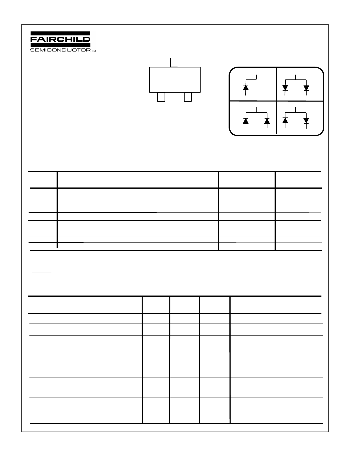
PACKAGE
SOT-23
3
L4P
CONNECTION DIAGRAMS
BAT54
3
3
BAT54A
TO-236AB (Low)
1 2
MARKING
1
BAT54C
2 NC
3
1
3
BAT54S
BAT54 L4P BAT54C L43
BAT54A L42 BAT54S L44
1
2
Schottky Barrier Diode
Sourced from Process KA
Absolute Maximum Ratings* TA = 25
Sym Parameter Value Units
T
stg
T
J
W
iv
I
F
i
f
i
F(surge)
P
D
Storage Temperature -55 to +150
Operating Junction Temperature +150 OC
Working Inverse Voltage 25 V
DC Forward Current (IF) 200 mA
Recurrent Peak Forward Current (IFRM) 300 mA
Peak Forward Surge Current (IFSM) Pulse Width = 1.0 Second 600 mA
Total Power Dissipation at 25OC 230 mW
Theta (R
th j-a) (Note 1) 430
O
C unless otherwise noted
O
O
C
K/W
2
21
*These ratings are limiting values above which the serviceability of any semiconductor device may be impaired
NOTES:
1) From junction to ambient mounted on a ceramic substrate of 10 mm x 8 mm x 0.6 mm
Electrical Characteristics TA = 25
O
C unless otherwise noted
SYM CHARACTERISTICS MIN MAX UNITS TEST CONDITIONS
B
I
V
Breakdown Voltage 30 V IR= 10 uA
V
Reverse Leakage 2.0 uA VR= 25 V
R
Forward Voltage 240 mV IF= 100 uA
F
320 mV IF= 1.0 mA
400 mV IF= 10 mA
500 mV IF= 30 mA
1.0 V IF= 100 mA
C
Capacitance 10 pF VR= 1.0 V
T
f = 1.0 MHz
T
Reverse Recovery Time 5.0 ns IF= IR = 10 mA
RR
IRR= 1.0 mA
RL = 100 Ohms
© 1997 Fairchild Semiconductor Corporation

BAT54
)
)
0.001
0.0001
0.00001
F
I - FORWARD CURRENT (A)
0.000001
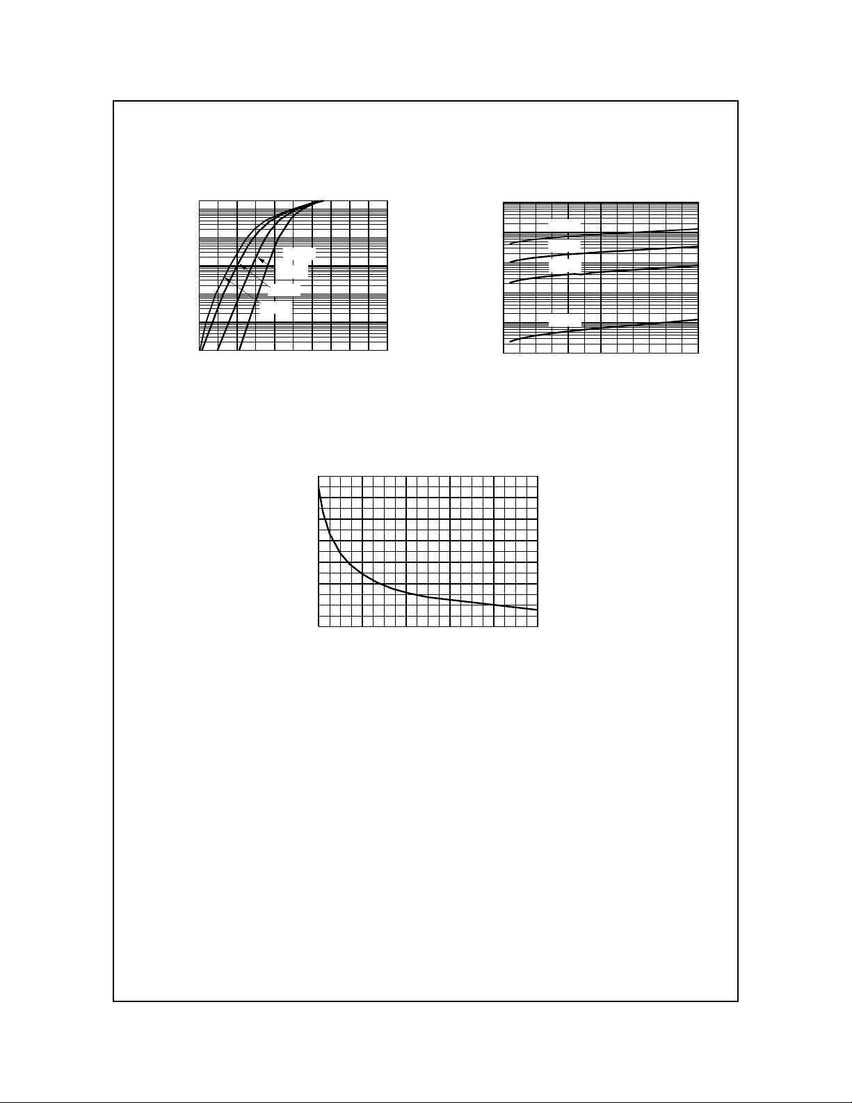
Forward Voltage
vs. Temper ature
0.2
0.1
0.01
75 C
100 C
25 C
o
o
-25 C
o
o
0 0.1 0.2 0.3 0.4 0.5 0.6 0.7 0.8 0.9 1
V - FORWARD VOLTAGE (V
vs. Reverse Bias Voltage
16
14
12
10
8
6
CAPACITANCE (pF)
4
2
012345678910
1
0.1
0.01
0.001
0.0001
0.00001
R
I - REVERSE LEAKAGE CURRENT (mA)
Capacitance
V - REVERSE BIAS VOLTAGE (V)
R
Reverse Leakage Current
vs. Temperature
o
125 C
o
100 C
o
75 C
o
25 C
0 5 10 15 20 25 30
V - REVERSE VOLTAGE (V
 Loading...