

Fairchild Semiconductor 9403APC Datasheet
9403A
First-In First-Out (FIFO) Buffer Memory
9403A First-In First-Out (FIFO) Buffer Memory
April 1989
Revised June 1999
General Description
The 9403A is an expandable fall-through type high-speed
First-In First-Out (FIFO) B uffer Memory optimized for high
speed disk or tape co ntrollers and communication buffer
applications. It is organized as 16 -wor ds by 4 -bit s and may
be expanded to any number of words or any number of bits
in multiples of four. Data may be entered or extracted asynchronously in serial or par allel, allowing econ omical i mplementation of buffer memories.
The 9403A has 3-STATE outputs which provide added versatility and is fully compatible with all TTL families.
Features
■ Serial or parallel input
■ Serial or parallel output
■ Expandable without external logic
■ 3-STATE outputs
■ Fully compatible with all TTL families
■ Slim 24-pin package
Ordering Code:
Order Number Package Number Package Description
9403APC N24E 24-Lead Plastic Dual-In-Line Package (PDIP), JEDEC MS-011, 0.400 Wide
Devices also availab le in Tape and Reel. Specify by appending the suffix letter “X” to the o rdering code.
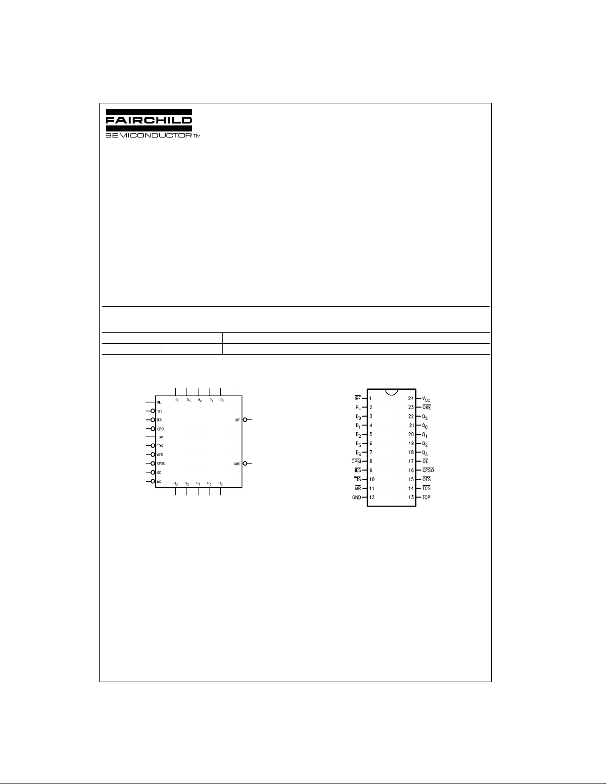
Logic Symbol Connection Diagram
© 1999 Fairchild Semiconductor Corporation DS010193.prf www.fairchildsemi.com
Unit Loading/Fan Out
9403A
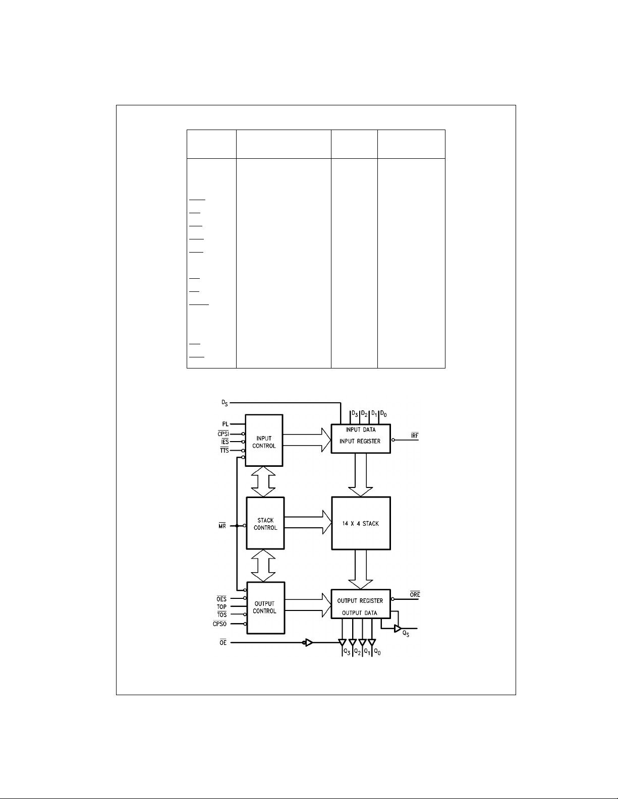
Block Diagram
Pin Names Description U.L. Input IIH/I
HIGH/LOW Output IOH/I
D0–D
8
D
S
P
L
CPSI
IES
TTS
OES
TOS
TOP Transfer Out Parallel 2.0/0.667 40 µA/400 µA
MR
OE
CPSO
- Q
Q
0
Q
S
IRF
ORE
Parallel Data Inputs 2.0/0.667 40 µA/400 µA
Serial Data Input 2.0/0.667 40 µA/400 µA
Parallel Load Input 2.0/0.667 40 µA/400 µA
Serial In put Clock 2.0/0.667 40 µA/400 µA
Serial In put Enable 2.0/0.66 7 40 µA/400 µA
Transfer to Stack Input 2.0/0.667 40 µA/400 µA
Serial Output Enable 2.0/0.667 40 µA/400 µA
Transfer Out Serial 2.0/0.667 40 µA/400 µA
Master Reset 2.0/0.667 40 µA/400 µA
Output Enable 2.0/0.667 40 µA/400 µA
Serial Output Clock 2.0/0.667 40 µA/400 µA
Parallel Data Outputs 285/26.7 5.7 mA/16 mA
3
Serial Data Output 285/26.7 5.7 mA/16 mA
Input Register Full 20/13.3 −400 µA/8 mA
Output Register Empty 20/13.3 −400 µA/8 mA
IL
OL
www.fairchildsemi.com 2
Functional Description
As shown in the block diagram the 49403A consists of
three sections:
1. An Input Register with parallel and serial data inputs as
well as control inputs and outputs for input handshaking and expansion.
2. A 4-bit wi de, 1 4-word deep fall- throu gh sta ck with se lfcontained control logic.
3. An Output Register with parallel and serial data outputs
as well as control inputs and ou tputs for output handshaking and expansion.
Since these three sections operate asynchronously and
almost independently, they will be described separately
below.
INPUT REGISTER (DATA ENTRY)
The Input Register can receive data in either bit-serial or in
4-bit parallel form. It stores this data until it is sent to the
fall-through stack and generates the necessa ry status a nd
control signals.
Figure 1 is a conceptual logic dia gram of th e inpu t section.
As described later, this 5-bit register is initialized by setting
the F
flip-flop and res ettin g t he oth er fl ip- flops. The Q out-
3
put of the last flip-fl op (FC) is brought out as the “Inpu t
Register Full” output (IRF
). After initialization this output is
HIGH.
Parallel Entry—A HIGH on the PL input loads the D
0-D3
inputs into the F0-F3 flip-flops and sets the FC flip-flop. This
forces the IRF
is full. During parallel entry, the CPSI
parallel expansi on is not be ing implem ented, IES
output LOW indicating that the input register
input must be LOW. If
must be
LOW to establish row mastership (see Expansion section).
Serial Entry—Data on the D
, F2, F1, F0, FC shift register on ea ch HIGH-to -LOW
the F
3
transition of the CPS I
input is serially entered into
S
clock input, provided IES a nd P L are
LOW.
After the fourth clock transition, the four data bits are
located in the four flip-flops, F
forcing the IRF
output LOW and interna lly inhibiting CPSI
. The FC flip-flop is set,
0-F3
clock pulses from affecting the reg ister, Figure 2 illustrates
the final positions in a 94 03A resulting fr om a 64-bit seri al
bit train. B
is the first bit, B63 the last bit.
0
9403A
FIGURE 1. Conceptual Input Section
FIGURE 2. Final Positions in a 9403A Resulting from a 64-Bit Serial Train
3 www.fairchildsemi.com

Transfer to the Stack—The outputs of Flip-Flops F0-F
feed the stack. A LO W level on the TTS input initiates a
“fall-through” action. If the top location of the stack is
9403A
empty, data is loaded into the stack and the input register is
re-initialized. Note that this initialization is postponed until
PL is LOW again. Thus, automatic FIFO action is achieved
by connecting the IRF
output to the TTS input.
An RS Flip-Flop (the Request Initialization Flip-Flop sho wn
in Figure 10) in the c ontrol section records the fact that
data has been transferred to the stack. This prevents multiple entry of the same word into the stac k despite the fact
and TTS may still be LOW. The Request Initializa-
the IRF
tion Flip-Flop is not cleared until PL goes LOW. Once in the
stack, data falls throu gh the stack automatically, pausing
3
only when it is necessary to wait for an empty next location.
In the 9403A as in most modern FIFO designs, the M R
input only initializes the stack contro l section and does not
clear the data.
OUTPUT REGISTER (DATA EXTRACTION)
The Output Register receives 4-bit data words from the
bottom stack location, stores it and outputs data on a 3STATE 4-bit parallel data bus or on a 3- STATE serial data
bus. The output section generates and receives the necessary status and cont rol signals. Figure 3 is a conceptual
logic diagram of the output section.
FIGURE 3. Conceptual Output Section
Parallel Data Extraction—When the FIFO is empty after a
LOW pulse is applied to MR
) output is LOW. After data has been en ter ed in to th e
(ORE
, the Output Register Empty
FIFO and has fallen through to the bottom stack location, it
is transferred into th e Output Register provid ed the “Transfer Out Parallel” (TOP) input is HIGH. As a result of the
data transfer O RE
goes HIGH, indicating valid da ta on the
data outputs (provided the 3-STATE buffer is enabled).
TOP can now be used to clock out the next word. When
TOP goes LOW, ORE
will go LOW indicating that the output data has been extracted, bu t the data itself rem ains on
the output bus until the next HIGH level at TOP permits the
transfer of the next wo rd (if a vailab le) in to the Ou tput Reg ister. During parallel data extraction CPSO
should be LOW.
TOS should be grounded for single slice operati on or con nected to the appropriate ORE
for expanded operation
(see Expansion section).
TOP is not edge triggered. Ther efore, if TOP goes HIGH
before data is available from the stack, but data does
become available befo re TOP goes LOW again , that data
will be transferred into the Output Register. However, internal control circuitry prevents the same data from being
www.fairchildsemi.com 4
transferred twice. If TOP goes HIGH and retur ns to LOW
before data is available fr om the sta ck, ORE
remains LOW
indicating that there is no valid data at the outputs.
Serial Data Extraction—When the FIFO is empty after a
LOW pulse is applied to MR
) output is LOW. After data has bee n e nte red into the
(ORE
, the Output Register Empty
FIFO and has fallen through to the bottom stack location, it
is transferred into the Output Register provided TOS
is
LOW and TOP is HIGH. As a result of the data trans fer
goes HIGH indicating valid data in the register. The 3-
ORE
STATE Serial Data Output, Q
, is automatically enabled
S
and puts the first data bit on the output bus. Data is serially
shifted out on the HIGH-to-LOW transition of CPSO
prevent false shifting, CPSO
should be LOW when the new
. To
word is being loaded into the Output Regist er. The fourth
transition empties the shift register, forces ORE
LOW and disables the serial output, Q
For serial operation the ORE
output may be tied to the TOS
(refer to Figure 3).
S
output
input, requesting a new word from the stack as soon as the
previous one has been shifted out.
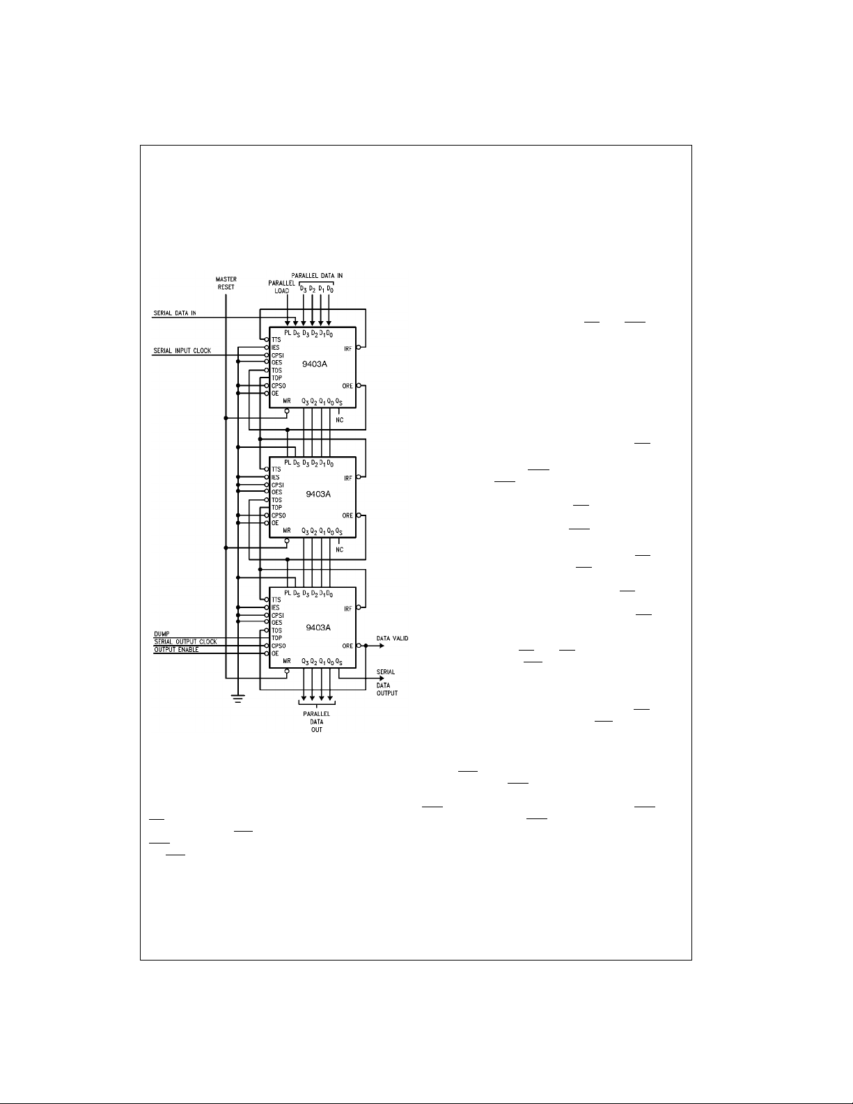
EXPANSION
Vertical Expansion—The 9403A may be vertically
expanded to store more words w ithout external par ts. The
interconnection is necessary to form a 46-word by 4-bit
FIFO are shown in Figur e 4. Using the same technique,
and FIFO of (15n + 1 )-word s by 4- bits can be constr ucted,
where n is the number of devices. Note that expansion
does not sacrifice any of the 9403A’s flexibility for serial/
parallel input and output.
FIGURE 4. A Vertical Expansion Scheme
Horizontal Expansion—The 9403A can also be horizontally expanded to store long words (in multiples of four bits)
without external logic. The interconnections necessar y to
form a 16-word by 12-bit FIFO are shown in Figure 5.
Using the same technique, any FIFO of 16 words by 4n bits
can be constructed, where n is the num ber of dev ices. T he
output of the right most device (most significant device)
IRF
is connected to the TTS
output of the most significan t device is connected to
ORE
inputs of all devices. As in the vertical expansion
the TOS
scheme, horizontal expansion does not sacrifice a ny of the
9403A’s flexibility for serial/parallel input and output.
inputs of all devices. Similarly, the
Horizontal and Vertical Expansion—The 9403A can be
expanded in both the horizontal and vertical directions
without any external pa rts and wi thou t sacrifici ng any of its
FIFO’s flexibility for serial/parallel input and output. The
interconnections necessary to form a 31-word by 16-bit
FIFO are shown in Figure 6 . Using the same technique,
any FIFO of (15m + 1)-words by (4n)-bits can be constructed, where m is the number of device s in a column
and n is the number of devices in a row. Figure 7 and Figure 8 show the timing d iagrams for serial data en try and
extraction for the 31-w ord by 16-bit FIFO show n in Figure
6. The final positio n o f dat a af ter serial insertion of 49 6 bi t s
into the FIFO array of Figure 6 is shown in Figure 9.
Interlocking Circuitry—Most conventual FIFO designs
provide status signal s analogous to IRF
ever, when these devices are operated in arrays, variations
in unit to unit o perating speed require externa l gating to
assure all devices have completed an operation. The
9403A incorporates simple but effective “master/slave”
interlocking circuitry to elimin ate the ne ed for ext ernal gating.
In the 9403A array of Figure 6 device s 1 and 5 a re defined
as “row masters” and the other devices are slaves to the
master in their row. No slave in a given row will initialize its
Input Register until it has received LOW on its IE S
from a row master or a slave of higher priority.
In a similar fash ion, the ORE
HIGH until their OES
locking scheme ensures that new input data may be
accepted by the array when the IRF
slave in that row goe s HIGH and that output data for the
array may be extracted when the ORE
the output row goes HIGH.
The row master is estab lished by connecting its IES
to ground while a slave receives it IES
output of the next higher prior ity device. When an ar ray of
9403A FIFOs is initialized with a LOW on the MR
all devices, the IRF outputs of all devices will be HIGH.
Thus, only the row master receives a LOW on the IES
during initialization. Figure 10 is a conceptual logic diagram
of the internal circuitry which determines master/slave
operation. Whenever MR
Latch is set. Whenever TTS
ization Flip-Flop will be set. If the Master Latch is HIGH, the
input Register will be immediately initialized and the
Request Initialization Flip-Flop reset. If the Mast er Latch is
reset, the Input Register is not initialized until IES
LOW. In array operation, activ ating the TTS
ple input register i nitialization from the row master to the
last slave.
A similar operation takes place for the output register.
Either a TOS
ation and sets the ORE
Latch is set, the last Output Register Flip-Fl op is set and
ORE
put will be LOW until an OES
or TOP input initiates a load-from-stack oper-
goes HIGH. If the Master latch is reset, the ORE out-
outputs of slaves will not go
inputs have gone HIGH. This inter-
and IES are LOW, the Master
goes LOW the Request Initial-
Request Flip-Flop. If the Master
input is received.
and ORE. How-
input
output of the final
of the final slave in
input
input from the IRF
inputs of
input
goes
initiates a rip-
9403A
5 www.fairchildsemi.com
 Loading...