

Fairchild Semiconductor 7824, 7806 Datasheet
©2001 Fairchild Semiconductor Corporation
www.fairchildsemi.com
Rev. 1.0.0
Features
• Output Current up to 1A
• Output Voltages of 5, 6, 8, 9, 10, 12, 15, 18, 24V
• Thermal Overload Protection
• Short Circuit Protection
• Output Transistor Safe Operating A r ea Protection
Description
The KA78XX/KA78XXA series of three-terminal positive
regulator are available in the TO-220/D-PAK package and
with several fix ed outp ut voltage s, makin g them usef ul in a
wide range of applications. Each type employs internal
current limiting, thermal shut down and safe operating area
protection , making it essen tially indestruc tible. If adequa te
heat sinking is provided, they can deliver over 1A output
current. Although de sig ne d pr i mar i ly as fi x e d volt age
regulators, these devices can be used with external
components to obtain adjustable voltages and currents.
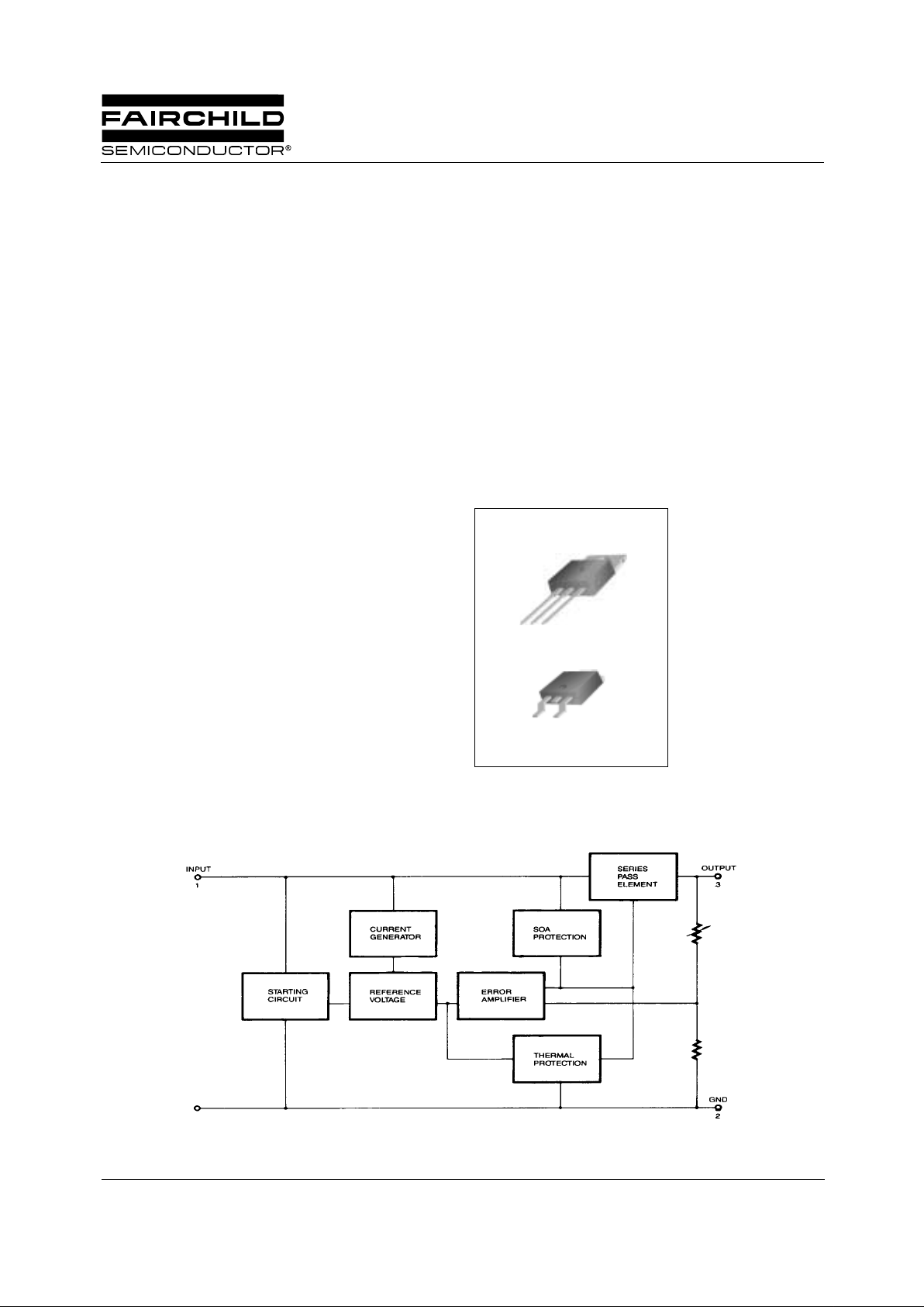
TO-220
D-PAK
1. Input 2. GND 3. Output
1
1
Internal Block Digram
KA78XX/KA78XXA
3-Terminal 1A Positiv e Voltage Regulator
KA78XX/KA78XXA
2
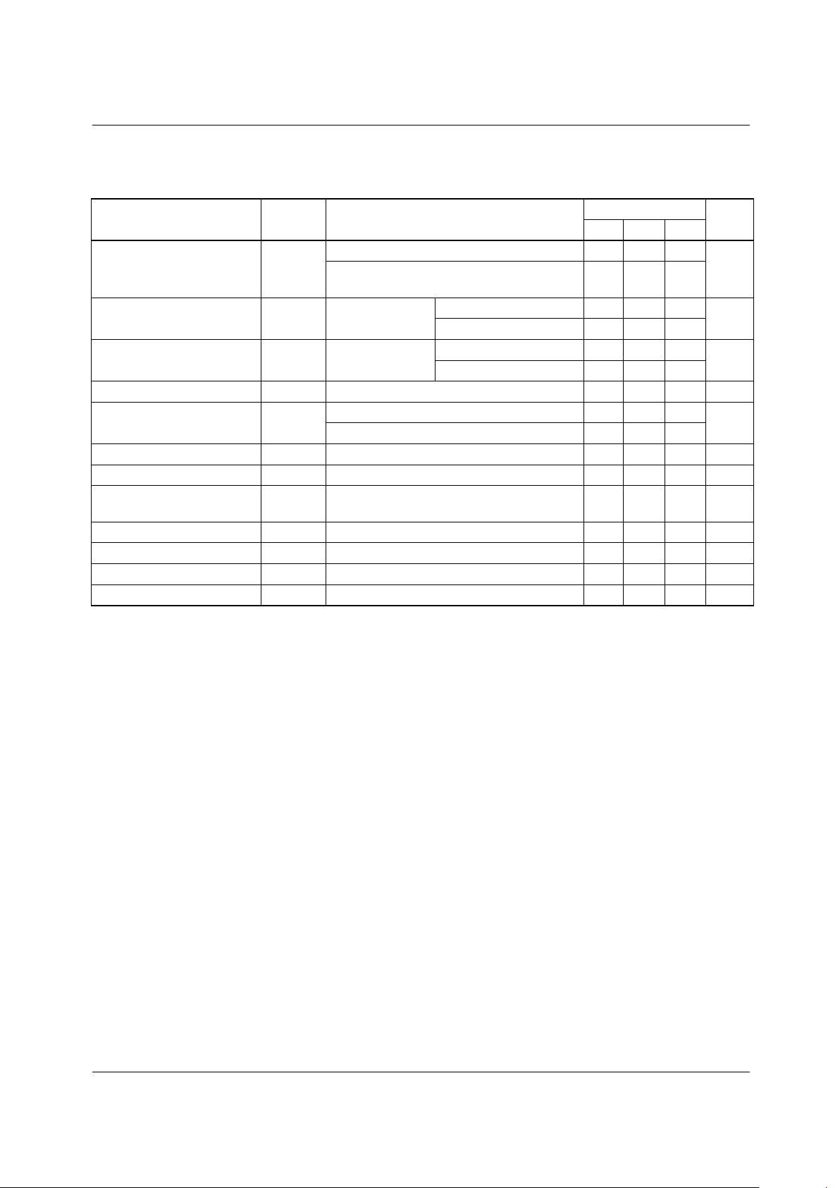
Absolute Maximum Ratings
Electrical Characteristics (KA7805/K A7805R)
(Refer to test circuit ,0°C < TJ < 125°C, IO = 500mA, VI =10V, CI= 0.33µF, CO=0.1µF, unless otherwis e specified)
Note:
1. Load and line regulation are specified at constant junction temperature. Changes in V
o
due to heatin g effe cts mus t be tak en
into account separately. Pulse testing with low duty is used.
Parameter Symbol Value Unit
Input Voltage (for V
O
= 5V to 18V)
(for V
O
= 24V)
V
I
V
I
35
40
V
V
Thermal Resistance Junction-Cases (TO-220) R
θJC
5
°
C/W
Thermal Resistance Junction-Air (TO-220) R
θJA
65
°
C/W
Operating Temperature Range (KA78XX/A/R) T
OPR
0 ~ +125
°
C
Storage Temperature Range T
STG
-65 ~ +150
°
C
Parameter Symbol Conditions
KA7805
Unit
Min. Typ. Max.
Output Voltage V
O
TJ =+25 oC 4.8 5.0 5.2
5.0mA ≤ Io ≤ 1.0A, P
O
≤ 15W
V
I
= 7V to 20V 4.75 5.0 5.25
V
Line Regulation (Note1) Regline T
J
=+25 oC
V
O
= 7V to 25V - 4.0 100
mV
V
I
= 8V to 12V - 1.6 50
Load Regulation (Note1) Regload T
J
=+25 oC
I
O
= 5.0mA to1.5A - 9 100
mV
I
O
=250mA to 750mA - 4 50
Quiescent Current I
Q
TJ =+25 oC-5.08.0mA
Quiescent Current Change ∆I
Q
IO = 5mA to 1.0A - 0.03 0.5
mA
V
I
= 7V to 25V - 0.3 1.3
Output Voltage Drift ∆V
O
/∆TIO= 5mA - -0.8 - mV/ oC
Output Noise Voltage V
N
f = 10Hz to 100KHz, TA=+25 oC-42-µV/V
O
Ripple Rejection RR
f = 120Hz
V
O
= 8V to 18V
62 73 - dB
Dropout Voltage V
Drop
IO = 1A, TJ =+25 oC-2-V
Output Resistance r
O
f = 1KHz - 15 - mΩ
Short Circuit Current I
SC
VI = 35V, TA =+25 oC - 230 - mA
Peak Current I
PK
TJ =+25 oC-2.2-A
KA78XX/KA78XXA
3
Electrical Characteristics (KA7806/K A7806R)
(Refer to test circuit ,0°C < TJ < 125°C, IO = 500mA, VI =11V, CI= 0.33µF, CO=0.1µF, unless otherwise specified)
Note:
1. Load and line regulation are specified at constant junction temperature. Changes in V
O
due to heating eff e cts mus t be t aken
into account separately. Pulse testing with low duty is used.
Parameter Symbol Conditions
KA7806
Unit
Min. Typ. Max.
Output Voltage V
O
TJ =+25 oC 5.75 6.0 6.25
5.0mA ≤ I
O
≤ 1.0A, PO≤ 15W
V
I
= 8.0V to 21V 5.7 6.0 6.3
V
Line Regulation (Note1) Regline T
J
=+25 oC
V
I
= 8V to 25V - 5 120
mV
V
I
= 9V to 13V - 1.5 60
Load Regulation (Note1) Regload T
J
=+25 oC
I
O
=5mA to 1.5A - 9 120
mV
I
O
=250mA to750mA - 3 60
Quiescent Current I
Q
TJ =+25 oC-5.08.0mA
Quiescent Current Change ∆I
Q
IO = 5mA to 1A - - 0.5
mA
V
I
= 8V to 25V - - 1.3
Output Voltage Drift ∆V
O
/∆TIO = 5mA - -0.8 -
mV/
o
C
Output Noise Voltage V
N
f = 10Hz to 100KHz, TA =+25 oC-45-µV/Vo
Ripple Rejection RR
f = 120Hz
V
I
= 9V to 19V
59 75 - dB
Dropout Voltage V
Drop
IO = 1A, TJ =+25 oC-2-V
Output Resistance r
O
f = 1KHz - 19 - mΩ
Short Circuit Current I
SC
VI= 35V, TA=+25 oC - 250 - mA
Peak Current I
PK
TJ =+25 oC-2.2-A
KA78XX/KA78XXA
4
Electrical Characteristics (KA7808/K A7808R)
(Refer to test circuit ,0°C < TJ < 125°C, IO = 500mA, VI =14V, CI= 0.33µF, CO=0.1µF, unless otherwis e specified)
Note:
1. Load and line regulation are specified at constant junction temperature. Changes in V
O
due to heating e ffe cts mus t be t ak en
into account separately. Pulse testing with low duty is used.
Parameter Symbol Conditions
KA7808
Unit
Min. Typ. Max.
Output Voltage V
O
TJ =+25 oC 7.7 8.0 8.3
5.0mA ≤ I
O
≤ 1.0A, PO≤ 15W
V
I
= 10.5V to 23V 7.6 8.0 8.4
V
Line Regulation (Note1) Regline T
J
=+25 oC
V
I
= 10.5V to 25V - 5.0 160
mV
V
I
= 11.5V to 17V - 2.0 80
Load Regulation (Note1) Regload TJ =+25 oC
I
O
= 5.0mA to 1.5A - 10 160
mV
I
O
= 250mA to
750mA
-5.080
Quiescent Current I
Q
TJ =+25 oC-5.08.0mA
Quiescent Current Change ∆I
Q
IO = 5mA to 1.0A - 0.05 0.5
mA
V
I
= 10.5A to 25V - 0.5 1.0
Output Voltage Drift ∆V
O
/∆TIO = 5mA - -0.8 - mV/ oC
Output Noise Voltage V
N
f = 10Hz to 100KHz, TA =+25 oC-52-µV/Vo
Ripple Rejection RR f = 120Hz, V
I
= 11.5V to 21.5V 56 73 - dB
Dropout Voltage V
Drop
IO = 1A, TJ=+25 oC-2-V
Output Resistance r
O
f = 1KHz - 17 - mΩ
Short Circuit Current I
SC
VI= 35V, TA =+25 oC - 230 - mA
Peak Current I
PK
TJ =+25 oC-2.2-A
KA78XX/KA78XXA
5
Electrical Characteristics (KA7809/K A7809R)
(Refer to test circuit ,0°C < TJ < 125°C, IO = 500mA, VI =15V, CI= 0.33µF, CO=0.1µF, unless otherwis e specified)
Note:
1. Load and line regulation are specified at constant junction temperature. Changes in V
O
due to heating eff e cts mus t be t aken
into account separately. Pulse testing with low duty is used.
Parameter Symbol Conditions
KA7809
Unit
Min. Typ. Max.
Output Voltage V
O
TJ =+25 oC 8.65 9 9.35
5.0mA≤ I
O
≤1.0A, PO ≤15W
V
I
= 11.5V to 24V 8.6 9 9.4
V
Line Regulation (Note1) Regline T
J
=+25 oC
V
I
= 11.5V to 25V - 6 180
mV
V
I
= 12V to 17V - 2 90
Load Regulation (Note1) Regload T
J
=+25 oC
I
O
= 5mA to 1.5A - 12 180
mV
I
O
= 250mA to 750mA - 4 90
Quiescent Current I
Q
TJ=+25 oC-5.08.0mA
Quiescent Current Change ∆I
Q
IO = 5mA to 1.0A - - 0.5
mA
V
I
= 11.5V to 26V - - 1.3
Output Voltage Drift ∆V
O
/∆TIO = 5mA - -1 - mV/ oC
Output Noise Voltage V
N
f = 10Hz to 100KHz, TA =+25 oC-58-µV/Vo
Ripple Rejection
RR
f = 120Hz
V
I
= 13V to 23V
56 71 - dB
Dropout Voltage V
DropIO
= 1A, TJ=+25 oC-2-V
Output Resistance r
O
f = 1KHz - 17 - mΩ
Short Circuit Current I
SC
VI= 35V, TA =+25 oC - 250 - mA
Peak Current I
PK
TJ= +25 oC-2.2-A

KA78XX/KA78XXA
6
Electrical Characteristics (KA7810)
(Refer to test circuit ,0°C < TJ < 125°C, IO = 500mA, VI =16V, CI= 0.33µF, CO=0.1µF, unless otherwis e specified)
Note:
1. Load and line regulation are specified at constant junction temperature. Changes in V
O
due to heating e ffe cts mus t be t ak en
into account separately. Pulse testing with low duty is used.
Parameter Symbol Conditions
KA7810
Unit
Min. Typ. Max.
Output Voltage V
O
TJ =+25 oC 9.6 10 10.4
5.0mA ≤ I
O
≤ 1.0A, PO ≤ 15W
V
I
= 12.5V to 25V 9.5 10 10.5
V
Line Regulation (Note1) Regline T
J
=+25 oC
V
I
= 12.5V to 25V - 10 200
mV
V
I
= 13V to 25V - 3 100
Load Regulation (Note1) Regload T
J
=+25 oC
I
O
= 5mA to 1.5A - 12 200
mV
I
O
= 250mA to 750mA - 4 400
Quiescent Current I
Q
TJ =+25 oC-5.18.0mA
Quiescent Current Change ∆I
Q
IO = 5mA to 1.0A - - 0.5
mA
V
I
= 12.5V to 29V - - 1.0
Output Voltage Drift ∆V
O
/∆TIO = 5mA - -1 - mV/ oC
Output Noise Voltage V
N
f = 10Hz to 100KHz, TA =+25 oC-58-µV/Vo
Ripple Rejection RR
f = 120Hz
V
I
= 13V to 23V
56 71 - dB
Dropout Voltage V
DropIO
= 1A, TJ=+25 oC-2-V
Output Resistance r
O
f = 1KHz - 17 - mΩ
Short Circuit Current I
SC
VI = 35V, TA=+25 oC - 250 - mA
Peak Current I
PK
TJ =+25 oC-2.2-A

KA78XX/KA78XXA
7
Electrical Characteristics (KA7812/K A7812R)
(Refer to test circuit ,0°C < TJ < 125°C, IO = 500mA, VI =19V, CI= 0.33µF, CO=0.1µF, unless otherwis e specified)
Note:
1. Load and line regulation are specified at constant junction temperature. Changes in V
O
due to heating e ffe cts mus t be t ak en
into account separately. Pulse testing with low duty is used.
Parameter Symbol Conditions
KA7812/KA7812R
Unit
Min. Typ. Max.
Output Voltage V
O
TJ =+25 oC 11.5 12 12.5
5.0mA ≤ I
O
≤1.0A, PO≤15W
V
I
= 14.5V to 27V 11.4 12 12.6
V
Line Regulation (Note1) Regline T
J
=+25 oC
V
I
= 14.5V to 30V - 10 240
mV
V
I
= 16V to 22V - 3.0 120
Load Regulation (Note1) Regload T
J
=+25 oC
I
O
= 5mA to 1.5A - 11 240
mV
I
O
= 250mA to 750mA - 5.0 120
Quiescent Current I
Q
TJ =+25 oC-5.18.0mA
Quiescent Current Change ∆I
Q
IO = 5mA to 1.0A - 0.1 0.5
mA
V
I
= 14.5V to 30V - 0.5 1.0
Output Voltage Drift ∆V
O
/∆TIO = 5mA - -1 - mV/ oC
Output Noise Voltage V
N
f = 10Hz to 100KHz, TA =+25 oC-76-µV/Vo
Ripple Rejection RR
f = 120Hz
V
I
= 15V to 25V
55 71 - dB
Dropout Voltage V
DropIO
= 1A, TJ=+25 oC-2-V
Output Resistance r
O
f = 1KHz - 18 - mΩ
Short Circuit Current I
SC
VI = 35V, TA=+25 oC - 230 - mA
Peak Current I
PK
TJ = +25 oC-2.2-A

KA78XX/KA78XXA
8
Electrical Characteristics (KA7815)
(Refer to test circuit ,0°C < TJ < 125°C, IO = 500mA, VI =23V, CI= 0.33µF, CO=0.1µF, unless otherwis e specified)
Note:
1. Load and line regulation are specified at constant junction temperature. Changes in V
O
due to heating eff e cts mus t be t aken
into account separately. Pulse testing with low duty is used.
Parameter Symbol Conditions
KA7815
Unit
Min. Typ. Max.
Output Voltage V
O
TJ =+25 oC 14.4 15 15.6
5.0mA ≤ I
O
≤1.0A, PO≤15W
V
I
= 17.5V to 30V 14.25 15 15.75
V
Line Regulation (Note1) Regline T
J
=+25 oC
V
I
= 17.5V to 30V - 11 300
mV
V
I
= 20V to 26V - 3 150
Load Regulation (Note1) Regload T
J
=+25 oC
I
O
= 5mA to 1.5A - 12 300
mV
I
O
= 250mA to 750mA - 4 150
Quiescent Current I
Q
TJ =+25 oC-5.28.0mA
Quiescent Current Change ∆I
Q
IO = 5mA to 1.0A - - 0.5
mA
V
I
= 17.5V to 30V - - 1.0
Output Voltage Drift ∆V
O
/∆TIO = 5mA - -1 - mV/ oC
Output Noise Voltage V
N
f = 10Hz to 100KHz, TA =+25 oC-90-µV/Vo
Ripple Rejection RR
f = 120Hz
V
I
= 18.5V to 28.5V
54 70 - dB
Dropout Voltage V
DropIO
= 1A, TJ=+25 oC-2-V
Output Resistance r
O
f = 1KHz - 19 - mΩ
Short Circuit Current I
SC
VI = 35V, TA=+25 oC - 250 - mA
Peak Current I
PK
TJ =+25 oC-2.2-A

KA78XX/KA78XXA
9
Electrical Characteristics (KA7818)
(Refer to test circuit ,0°C < TJ < 125°C, IO = 500mA, VI =27V, CI= 0.33µF, CO=0.1µF, unless otherwis e specified)
Note:
1. Load and line regulation are specified at constant junction temperature. Changes in V
O
due to heating e ffe cts mus t be t ak en
into account separately. Pulse testing with low duty is used.
Parameter Symbol Conditions
KA7818
Unit
Min. Typ. Max.
Output Voltage V
O
TJ =+25 oC 17.3 18 18.7
5.0mA ≤ I
O
≤1.0A, PO ≤15W
V
I
= 21V to 33V 17.1 18 18.9
V
Line Regulation (Note1) Regline T
J
=+25 oC
V
I
= 21V to 33V - 15 360
mV
V
I
= 24V to 30V - 5 180
Load Regulation (Note1) Regload T
J
=+25 oC
I
O
= 5mA to 1.5A - 15 360
mV
I
O
= 250mA to 750mA - 5.0 180
Quiescent Current I
Q
TJ =+25 oC-5.28.0mA
Quiescent Current Change ∆I
Q
IO = 5mA to 1.0A - - 0.5
mA
V
I
= 21V to 33V - - 1
Output Voltage Drift ∆V
O
/∆TIO = 5mA - -1 - mV/ oC
Output Noise Voltage V
N
f = 10Hz to 100KHz, TA =+25 oC-110-µV/Vo
Ripple Rejection RR
f = 120Hz
V
I
= 22V to 32V
53 69 - dB
Dropout Voltage V
DropIO
= 1A, TJ=+25 oC - 2 - V
Output Resistance r
O
f = 1KHz - 22 - mΩ
Short Circuit Current I
SC
VI = 35V, TA=+25 oC - 250 - mA
Peak Current I
PK
TJ =+25 oC-2.2-A
 Loading...