

Fairchild Semiconductor 74VHCU04N, 74VHCU04MX, 74VHCU04MTCX, 74VHCU04MTC, 74VHCU04MSCX Datasheet
...
July 1993
Revised April 1999
74VHCU04 Hex Inverter
© 1999 Fairchild Semiconductor Corporation DS011626.prf www.fairchildsemi.com
74VHCU04
Hex Inverter
General Description
The VHCU04 is an advanced high speed CMOS Inverter
fabricated with silicon gate CMOS technology. It achieves
the high speed operation similar to equivalent Bipolar
Schottky TTL while maintaining the CMOS low power dissipation.
Since the internal circuit is composed of a single stage
inverter, it can be used in analog applications such as crystal oscillators. An input protection circuit ensures that 0V to
7V can be applied to t he input pins without r egard to the
supply voltage. This dev ice can be used to interf ace 5V to
3V systems and two supply systems such as battery
backup. Thi s ci r c ui t pr ev ent s d e vi ce d est r uc ti o n du e to m is matched supply and input voltages.
Features
■ High Speed: tPD = 3.5 ns (typ) at VCC = 5V
■ Low Power Dissipation: I
CC
= 2 µA (Max) @ TA = 25°C
■ High Noise Immunity: V
NIH
= V
NIL
= 28% VCC (Min)
■ Power down protection is provided on all inputs
■ Low Noise: V
OLP
= 0.8V (Max)
■ Pin and Function Compatible with 74HCU04
Ordering Code:
Surface mount pack ages are also available on Tape and Reel. Specify by appending the s uffix let te r “X” to the ordering code.
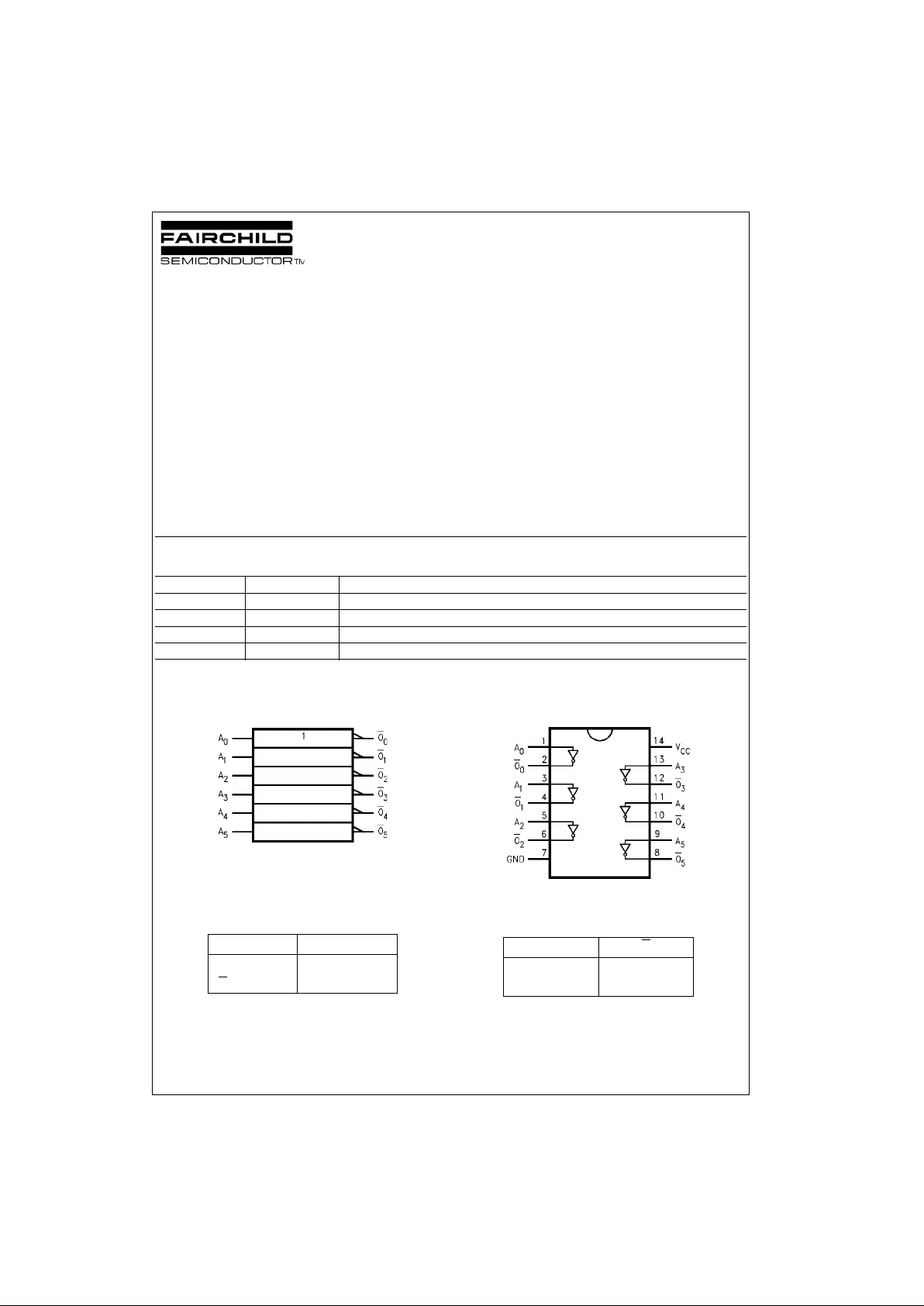
Logic Symbol
IEEE/IEC
Pin Descriptions
Connection Diagram
Truth T able
Order Number Package Number Package Description
74VHCU04M M14A 14-Lead Small Outline Integrated Circuit (SOIC), JEDEC MS-120, 0.150 Narrow
74VHCU04SJ M14D 14-Lead Small Outline Package (SOP), EIAJ TYPE II, 5.3mm Wide
74VHCU04MTC MTC14 14-Lead Thin Shrink Small Outline Package (TSSOP), JEDEC MO-153, 4.4mm Wide
74VHCU04N N14A 14-Lead Plastic Dual-In-Line Package (PDIP), JEDEC MS-001, 0.300 Wide
Pin Names Description
A
n
Inputs
O
n
Outputs
AO
LH
HL
www.fairchildsemi.com 2
74VHCU04
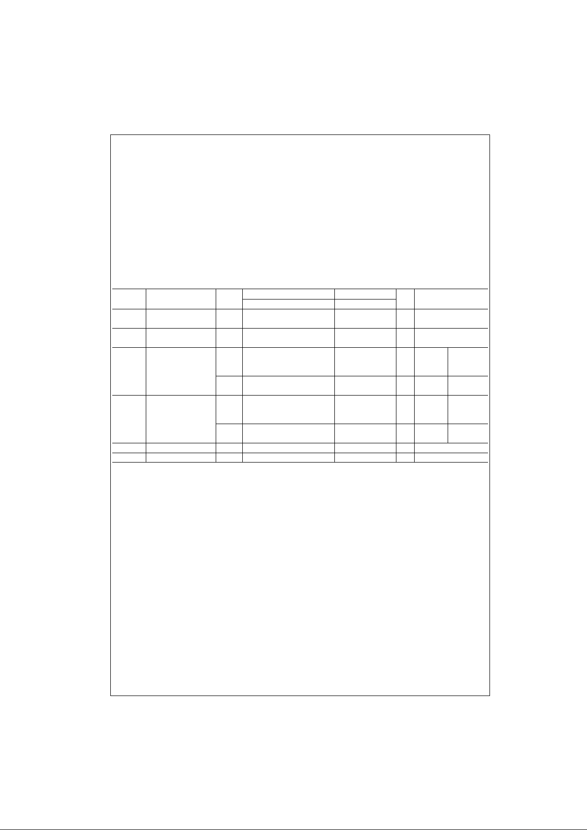
Absolute Maximum Ratings(Note 1) Recommended Operating
Conditions
(Note 2)
Note 1: Absolute Maximum Ratings are values beyond which the device
may be damaged or ha ve its useful li fe impaire d. The datab ook specifications should be met, without exception, to ensure that the system design is
reliable over its p ower supp ly, temperature, and ou tput/input loading variables. Fairchild does not recom mend operation outs ide databook specifications.
Note 2: Unused inputs must be held HIGH or LOW. They may not float.
DC Electrical Characteristics
Supply Voltage (VCC) −0.5V to +7.0V
DC Input Voltage (V
IN
) −0.5V to +7.0V
DC Output Voltage (V
OUT
) −0.5V to VCC + 0.5V
Input Diode Current (I
IK
) −20 mA
Output Diode Current (I
OK
) ±20 mA
DC Output Current (I
OUT
) ±25 mA
DC V
CC
/GND Current (ICC) ±50 mA
Storage Temperature (T
STG
) −65°C to +150°C
Lead Temperature (T
L
)
(Soldering, 10 seconds) 260°C
Supply Voltage (V
CC
) 2.0V to +5.5V
Input Voltage (V
IN
)0V to +5.5V
Output Voltage (V
OUT
)0V to V
CC
Operating Temperature (T
OPR
) −40°C to +85°C
Symbol Parameter
V
CC
(V)
TA = 25°CT
A
= −40°C to +85°C
Units Conditions
Min Typ Max Min Max
V
IH
HIGH Level 2.0 1.70 1.70
V
Input Voltage 3.0 − 5.5 0.8 V
CC
0.8 V
CC
V
IL
LOW Level 2.0 0.30 0.30
V
Input Voltage 3.0 − 5.5 0.20 V
CC
0.20 V
CC
V
OH
HIGH Level 2.0 1.8 2.0 1.8 VIN = VILIOH = −50 µA
Output Voltage 3.0 2.7 3.0 2.7 V
4.5 4.0 4.5 4.0
3.0 2.58 2.48
V
VIN = GND IOH = −4 mA
4.5 3.94 3.80 IOH = −8 mA
V
OL
LOW Level 2.0 0.0 0.2 0.2 VIN = VIHIOL = 50 µA
Output Voltage 3.0 0.0 0.3 0.3 V
4.5 0.0 0.5 0.5
3.0 0.36 0.44
V
VIN = VCCIOL = 4 mA
4.5 0.36 0.44 IOL = 8 mA
I
IN
Input Leakage Current 0 − 5.5 ±0.1 ±1.0 µAVIN = 5.5V or GND
I
CC
Quiescent Supply Current 5.5 2.0 20.0 µAVIN = VCC or GND
 Loading...