

Fairchild Semiconductor 74VHCT74AMTCX, 74VHCT74AMTC, 74VHCT74AM, 74VHCT74ACW, 74VHCT74ASJX Datasheet
...
July 1997
Revised April 1999
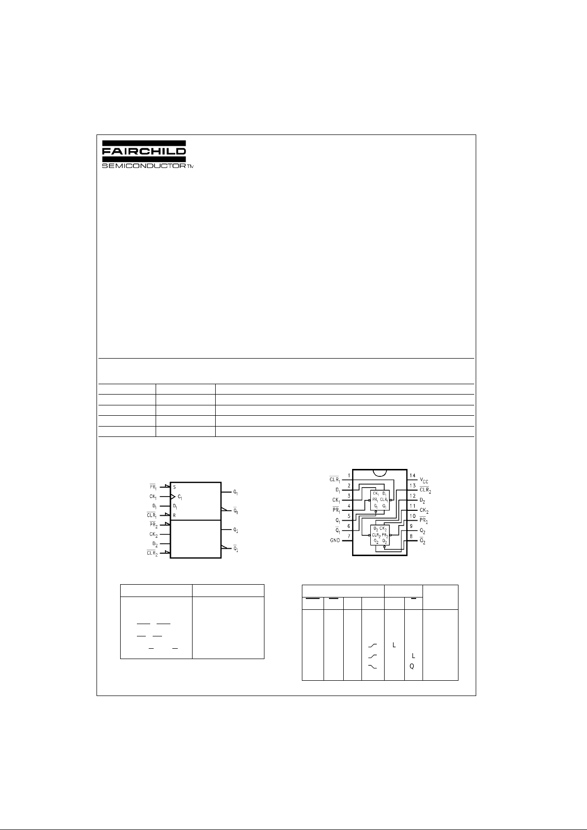
74VHCT74A Dual D-Type Flip-Flop with Preset and Clear
© 1999 Fairchild Semiconductor Corporation DS500026.prf www.fairchildsemi.com
74VHCT74A
Dual D-Type Flip-Flop with Preset and Clear
General Description
The VHCT74A is an advance d high speed CMOS Dual D Type Flip-Flop fabricated with silicon gate CMOS technology. It achieves the high speed operation similar to equivalent Bipolar Schottky TTL while maintaining the CMOS low
power dissipation. The sig nal level applied to the D IN PUT
is transferred to the Q OUTPU T during the positive goi ng
transition of the CK pulse. CLR and PR are inde pen den t of
the CK and are accompl ished by setting the appropria te
input LOW.
Protection circuits ensu re that 0V to 7V can be applied to
the input pins without reg ard to the supply voltage an d to
the output pins with V
CC
= 0V. These circuits prevent
device destruction due to m ismatched supply and input/
output voltages. This device ca n be used to interface 3V to
5V systems and two supply systems such as battery
backup.
Features
■ High spee d: f
MAX
= 160 MHz (typ) at TA= 25°C
■ High noise immunity: V
IH
= 2.0V, VIL = 0.8V
■ Power down protection is provided on all inputs and
outputs
■ Low power dissipation:
I
CC
= 2 µA (max) at TA= 25°C
■ Pin and function compatible with 74HCT74
Ordering Code:
Surface mount pack ages are also available on Tape and Reel. Specify by appending the s uffix let te r “X” to the ordering code.
Logic Symbol
IEEE/IEC
Pin Descriptions
Connection Diagram
Truth Table
Order Number Package Number Package Description
74VHCT74AM M14A 14-Lead Small Outline Integrated Circuit (SOIC), JEDEC MS-120, 0.150 Narrow
74VHCT74ASJ M14D 14-Lead Small Outline Package (SOP), EIAJ TYPE II, 5.3mm Wide
74VHCT74AMTC MTC14 14-Lead Thin Shrink Small Outline Package (TSSOP), JEDEC MO-153, 4.4mm Wide
74VHCT74AN N14A 14-Lead Plastic Dual-In-Line Package (PDIP), JEDEC MS-001, 0.300 Wide
Pin Names Description
D
1
, D
2
Data Inputs
CK
1
, CK
2
Clock Pulse Inputs
CLR
1
, CLR
2
Direct Clear Inputs
PR
1
, PR
2
Direct Preset Inputs
Q
1
, Q1, Q2, Q
2
Outputs
Inputs Outputs
Function
CLR
PR DCKQQ
L H X X L H Clear
HLXXHLPreset
LLXXHH
HHL
LH
HHH
HL
HHX
QnQnNo
Change
www.fairchildsemi.com 2
74VHCT74A
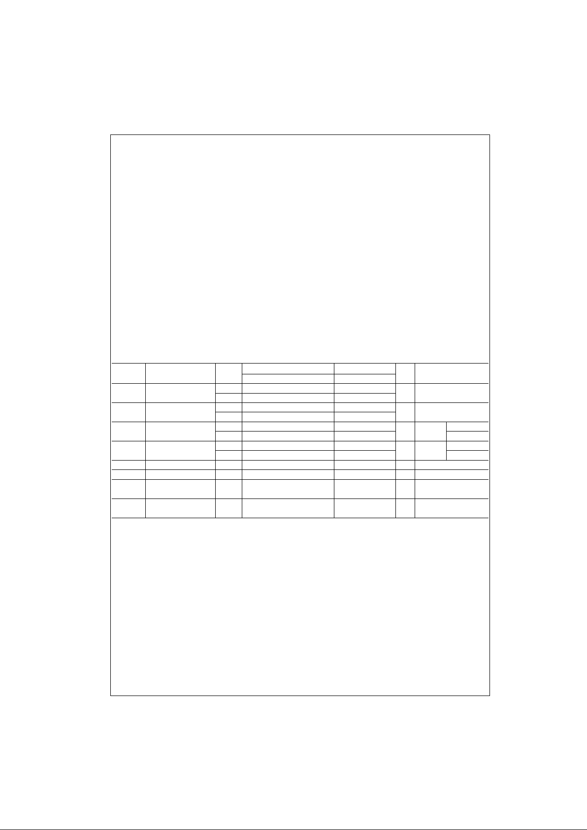
Absolute Maximum Ratings(Note 1) Recommended Operating
Conditions
(Note 5)
Note 1: Absolute maximum ratings are values beyond which the device
may be damaged or ha ve its useful li fe impaire d. The datab ook specifications should be met, without exception, to ensure that the system design is
reliable over its power sup ply, temperature, and outpu t/input lo ading var aibles. Fairchild does not reco mmend ope ration outsid e databook sp ecifications.
Note 2: HIGH or LOW state. I
OUT
absolute maximum rating must be
observed.
Note 3: V
CC
= 0V.
Note 4: V
OUT
< GND, V
OUT
> VCC.(Outputs Active)
Note 5: Unused inputs must be held HIGH or LOW. They may not float.
DC Electrical Characteristics
Supply Voltage (VCC) −0.5V to +7.0V
DC Input Voltage (V
IN
) −0.5V to +7.0V
DC Output Voltage (V
OUT
)
(Note 2) −0.5V to V
CC
+ 0.5V
(Note 3) −0.5V to 7.0V
Input Diode Current (I
IK
) −20 mA
Output Diode Current (I
OK
)
(Note 4) ±20 mA
DC Output Current (I
OUT
) ±25 mA
DC V
CC
/GND Current (ICC) ±50 mA
Storage Temperature (T
STG
) −65°C to +150°C
Lead Temperature (T
L
)
Solderin g (10 seconds) 260°C
Supply Voltage (V
CC
) 4.5V to 5.5V
Input Voltage (V
IN
)0V to +5.5V
Output Voltage (V
OUT
)
(Note 2) 0V to V
CC
(Note 3) 0V to 5.5V
Operating Temperature (T
OPR
) −40°C to +85°C
Input Rise and Fall Time (t
r
, tf)
V
CC
= 5.0V ± 0.5V 0 ns/V ∼ 20 ns/V
Symbol Parameter
V
CC
(V)
TA = 25°CT
A
= −40°C to +85°C
Units Conditions
Min Typ Max Min Max
V
IH
HIGH Level 4.5 2.0 2.0
V
Input Voltage 5.5 2.0 2.0
V
IL
LOW Level 4.5 0.8 0.8
V
Input Voltage 5.5 0.8 0.8
V
OH
HIGH Level 4.5 4.40 4.50 4.40
V
VIN = VIHIOH = −50 µA
Output Voltage 4.5 3.94 3.80 or VILIOH = −8 mA
V
OL
LOW Level 4.5 0.0 0.1 0.1
V
VIN = VIHIOL = 50 µA
Output Voltage 4.5 0.36 0.44 or VILIOL = 8 mA
I
IN
Input Leakage Current 0–5.5 ±0.1 ±1.0 µAVIN = 5.5V or GND
I
CC
Quiescent Supply Current 5.5 2.0 20.0 µAVIN = VCC or GND
I
CCT
Maximum ICC/Input
5.5 1.35 1.50 mA
VIN = 3.4V
Other Inputs = VCC or GND
I
OFF
Output Leakage Current 0.0 +0.5 +5.0 µAV
OUT
= 5.5V
(Power Down State)
 Loading...