


Fairchild Semiconductor 74VHCT574ASJX, 74VHCT574ASJ, 74VHCT574AN, 74VHCT574AMX, 74VHCT574AMTCX Datasheet
...
July 1997
Revised April 1999
74VHCT574A Octal D-Type Flip-Flop with 3-STATE Outputs
© 1999 Fairchild Semiconductor Corporation DS500029.prf www.fairchildsemi.com
74VHCT574A
Octal D-Type Flip-Flop with 3-STATE Outputs
General Description
The VHCT574A is an advanced high speed CM OS octal
flip-flop with 3-STATE output fabricated with silicon gate
CMOS technology. It achieves the high speed operation
similar to equivalent Bipolar Schottky TTL while maintaining the CMOS low power dissipation. This 8-b it D -type f lipflop is controlled by a clock input (CP) and an Output
Enable input (OE
). When the OE input is HIGH, the eight
outputs are in a high impedance state.
Protection circuits ensu re that 0V to 7V can be applied to
the input and output (No te 1) pins without regard to the
supply voltage. This dev ice can be used to interf ace 3V to
5V systems and two supply systems such as batter y back
up. This circuit prevents device destruction due to mismatched supply and input voltages.
Note 1: Outputs in OFF-State.
Features
■ High speed: f
MAX
= 140 MHz (typ) at TA = 25°C
■ Power Down Protection is provided on all inputs and
outputs.
■ Low Noise: V
OLP
= 1.6V (max)
■ Low Power Dissipation:
I
CC
= 4 µA (max) @ TA = 25°C
■ Pin and Function Compatible with 74HCT574
Ordering Code:
Surface mount pack ages are also available on Tape and Reel. Specify by appending the s uffix let te r “X” to the ordering code.
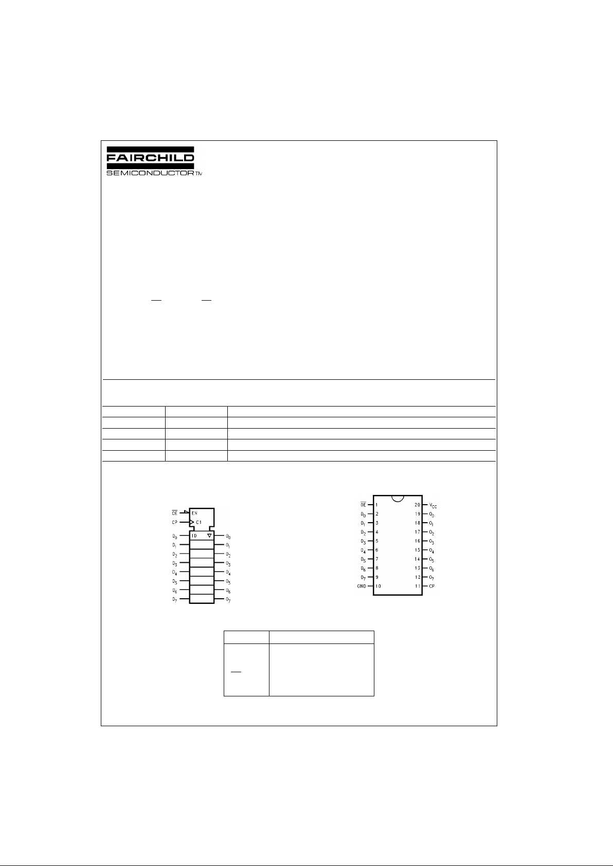
Logic Symbol
IEEE/IEC
Connection Diagram
Pin Descriptions
Order Number Package Number Package Description
74VHCT574AM M20B 20-Lead Small Outline Integrated Circuit (SOIC), JEDEC MS-013, 0.300 Wide
74VHCT574ASJ M20D 20-Lead Small Outline Package (SOP), EIAJ TYPE II, 5.3mm Wide
74VHCT574AMTC MTC20 20-Lead Thin Shrink Small Outline Package (TSSOP), JEDEC MO-153, 4.4mm Wide
74VHCT574AN N20A 20-Lead Plastic Dual-In-Line Package (PDIP), JEDEC MS-001, 0.300 Wide
Pin Names Description
D
0–D7
Data Inputs
CP Clock Pulse Input 3-STATE
OE
Output Enable Input 3-STATE
O
0–O7
Outputs
www.fairchildsemi.com 2
74VHCT574A
Functional Description
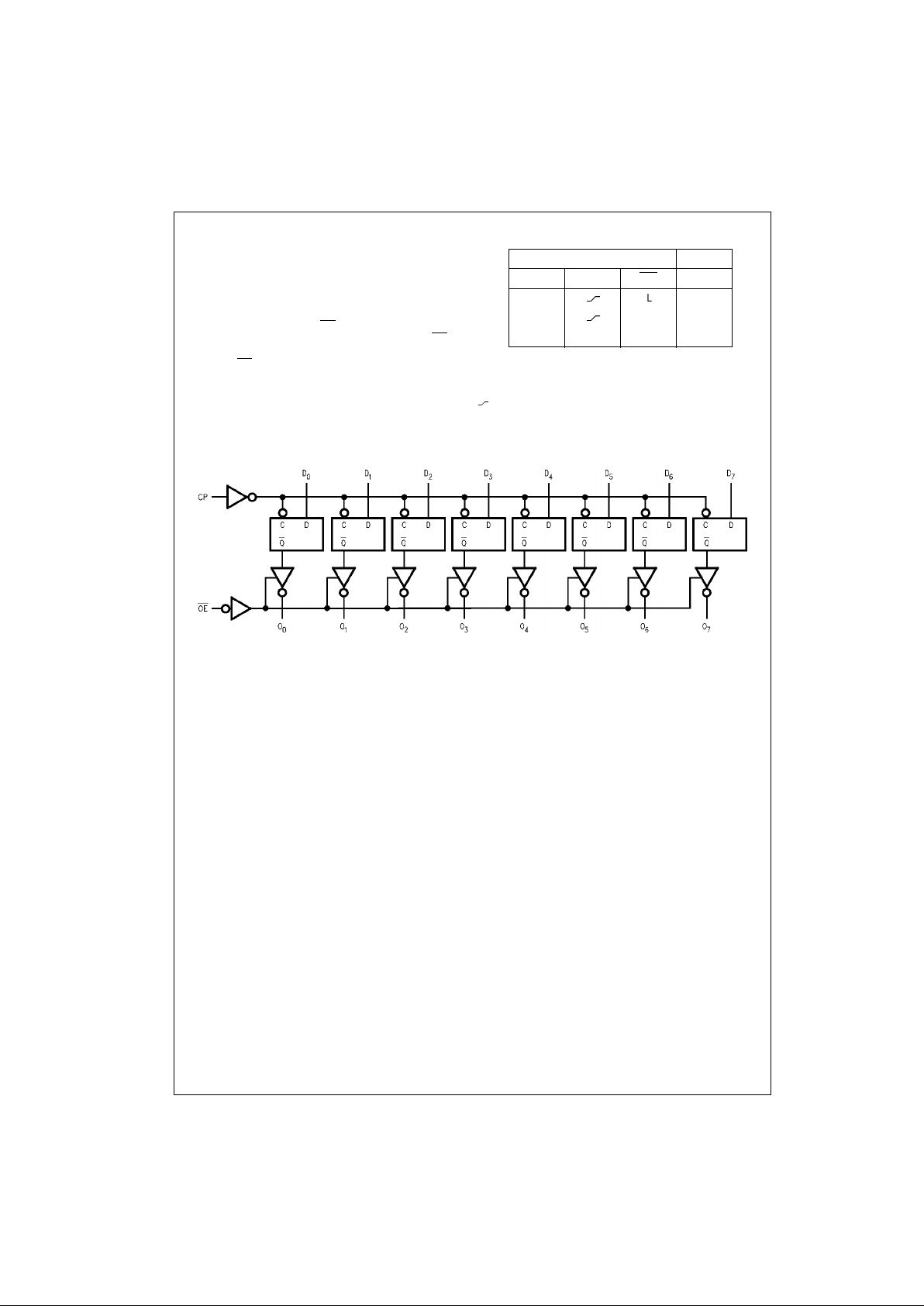
The VHCT574A co nsists of eight ed ge-triggered flip-flo ps
with individual D-type inputs and 3-STATE true outputs.
The buffered clock and buffered Output Enable are common to all flip-flops. The eight flip-flops will store the sta te
of their individual D inp uts that meet the setup and hold
time requirement s on the LO W-to-HIG H Cloc k (C P) tran sition. With the Output Enable (OE
) LOW, th e cont e nt s of t he
eight flip-flops are available at the outputs. When the OE
is
HIGH, the outputs go to th e high impeda nce state. Op eration of the OE
input does not affect t he state of the flip-
flops.
Tr uth Table
H = HIGH Voltage Level
L = LOW Voltage Level
X = Immaterial
Z = High Impedance
= LOW-to-HIGH Transition
Logic Diagram
Please note that this diagram is provided only f or t he understanding of logic operations and should not be used to estimate propagation delays.
Inputs Outputs
D
n
CP OE O
n
H
L H
L
L L
X X H Z
3 www.fairchildsemi.com
74VHCT574A
Absolute Maximum Ratings(Note 2) Recommended Operating
Conditions
(Note 6)
Note 2: Absolute Maximum Ratings are valu es beyond whic h the device
may be damaged or ha ve its useful life impaire d. The datab ook specifications should be met, without exception, to ensure that the system design is
reliable over its p ower supp ly, temperature, and o utput/input loading variables. Fairchild does not recommend operation outside databook specifications.
Note 3: HIGH or LOW state. I
OUT
absolute maximum rating must be
observed.
Note 4: When outputs are in OFF-S ta t e or w hen V
CC
= OV.
Note 5: V
OUT
< GND, V
OUT
> VCC (Outputs Active).
Note 6: Unused inputs must be held HIGH or LOW. They may not float.
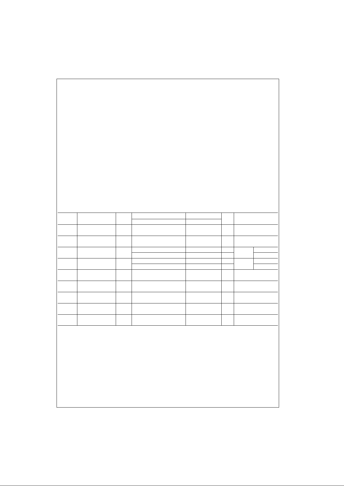
DC Electrical Characteristics
Supply Voltage (VCC) −0.5V to +7.0V
DC Input Voltage (V
IN
) −0.5V to +7.0V
DC Output Voltage (V
OUT
)
(Note 3) −0.5V to V
CC
+ 0.5V
(Note 4) −0.5V to +7.0V
Input Diode Current (I
IK
) −20 mA
Output Diode Current (I
OK
) (Note 5) ±20 mA
DC Output Current (I
OUT
) ±25 mA
DC V
CC
/GND Current (ICC) ±75 mA
Storage Temperature (T
STG
) −65°C to +150°C
Lead Temperature (T
L
)
(Solderi ng, 10 seconds) 260°C
Supply Voltage (V
CC
) 4.5V to +5.5V
Input Voltage (V
IN
) 0V to +5.5V
Output Voltage (V
OUT
)
(Note 3) 0V to V
CC
(Note 4) 0V to +5.5V
Operating Temperature (T
OPR
) −40°C to +85°C
Input Rise and Fall Time (t
r
, tf)
V
CC
= 5.0V ± 0.5V 0 ns/V ∼ 20 ns/V
Symbol Parameter
V
CC
(V)
TA = 25°CT
A
= −40°C to +85°C
Units Conditions
Min Typ Max Min Max
V
IH
HIGH Level 4.5 2.0 2.0
V
Input Voltage 5.5 2.0 20
V
IL
LOW Level 4.5 0.8 0.8
V
Input Voltage 5.5 0.8 0.8
V
OH
HIGH Level
4.5
4.40 4.50 4.40 V VIN = VIHIOH = −50 µA
Output Voltage 3.94 3.80 V or VILIOH = −8 mA
V
OL
LOW Level
4.5
0.0 0.1 0.1 V VIN = VIHIOL = 50 µA
Output Voltage 0.36 0.44 V or VILIOL = 8 mA
I
OZ
3-STATE Output
5.5 ±0.25 ±2.5 µA
VIN = VIH or V
IL
Off-State Current V
OUT
= VCC or GND
I
IN
Input Leakage
0–5.5 ±0.1 ±1.0 µA
VIN = 5.5V or GND
Current
I
CC
Quiescent Supply
5.5 4.0 40.0 µA
VIN = VCC or GND
Current
I
CCT
Maximum ICC/Input
5.5 1.35 1.50 mA
VIN = 3.4V
Other Input = VCC or GND
I
OFF
Output Leakage Current
0.0 0.5 5.0 µA
V
OUT
= 5.5V
(Power Down State)