

Fairchild Semiconductor 74VHCT573ASJ, 74VHCT573AN, 74VHCT573AMX, 74VHCT573AMTCX, 74VHCT573AMTC Datasheet
...
January 1998
Revised April 1999
74VHCT573A Octal D-Type Latch with 3-STATE Outputs
© 1999 Fairchild Semiconductor Corporation DS500028.prf www.fairchildsemi.com
74VHCT573A
Octal D-Type Latch with 3-STATE Outputs
General Description
The VHCT573A is an advanced high speed CM OS octal
latch with 3-STATE output fabricated with silicon gate
CMOS technology. It achieves the high speed operation
similar to equivalent Bipolar Schottky TTL while maintaining the CMOS low power dissipation. This 8-bit D-type
latch is controlled by a Latch Enable input (LE) and an Output Enable input (OE
). When the OE input is HIGH, t he
eight outputs are in a high impedance state.
Protection circuits ensu re that 0V to 7V can be applied to
the input and output (No te 1) pins without regard to the
supply voltage. This dev ice can be used to interf ace 3V to
5V systems and two supply systems such as batter y back
up. This circuit prevents device destruction due to mismatched supply and input voltages.
Note 1: Outputs in OFF-State.
Features
■ High speed: tPD = 7.7 ns (typ) at TA = 25°C
■ High Noise Immunity: V
IH
= 2.0V, VIL = 0.8V
■ Power Down Protection is provided on all inputs and
outputs
■ Low Noise: V
OLP
= 1.6V (max)
■ Low Power Dissipation:
I
CC
= 4 µA (max) @ TA = 25°C
■ Pin and function compatible with 74HCT573
Ordering Code:
Surface mount pack ages are also available on Tape and Reel. Specify by appending the s uffix let te r “X” to the ordering code .
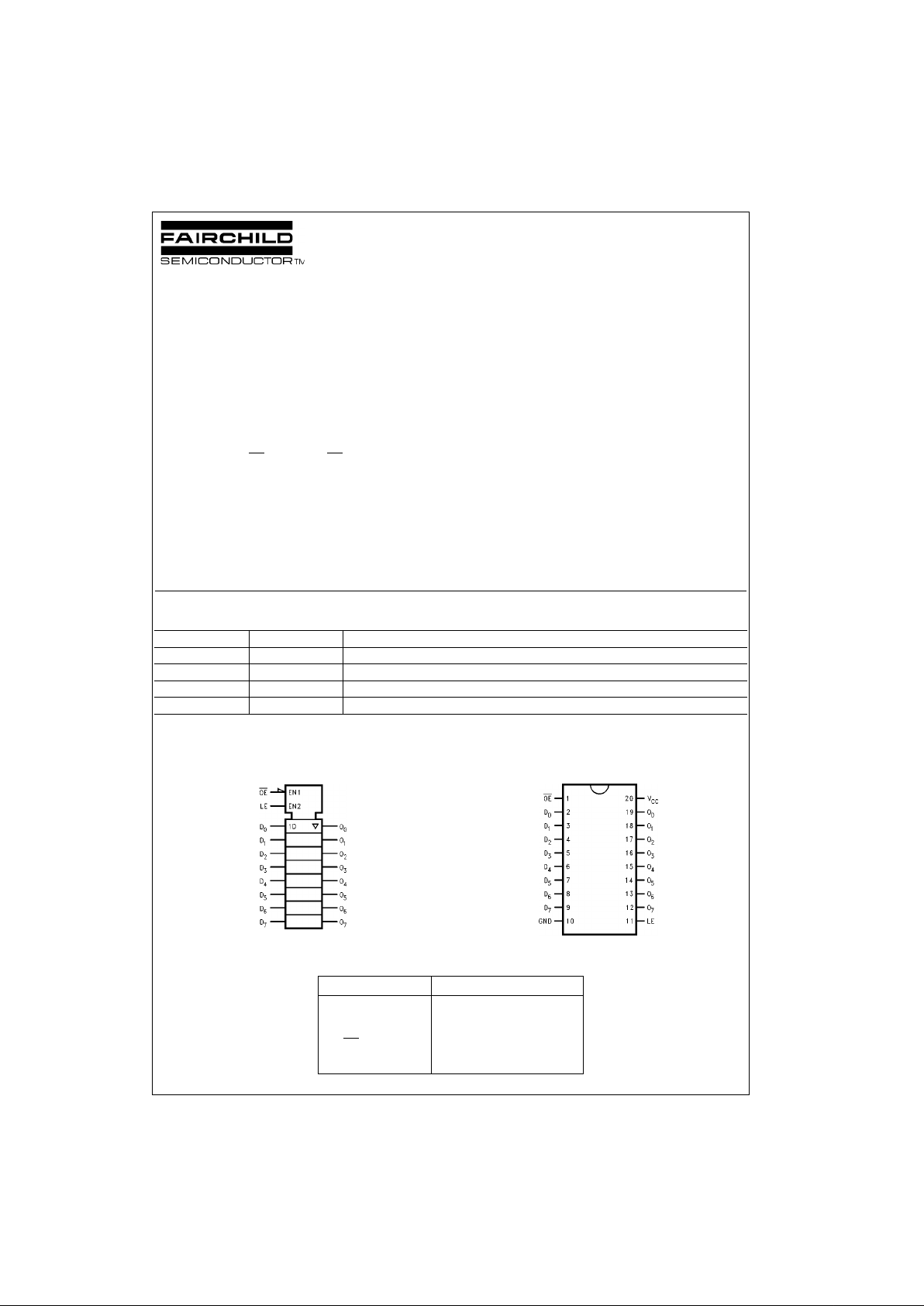
Logic Symbol
IEEE/IEC
Connection Diagram
Pin Descriptions
Order Number Package Number Package Description
74VHCT573AM M20B 20-Lead Small Outline Integrated Circuit (SOIC), JEDEC MS-013, 0.300 Wide
74VHCT573ASJ M20D 20-Lead Small Outline Package (SOP), EIAJ TYPE II, 5.3mm Wide
74VHCT573AMTC MTC20 20-Lead Thin Shrink Small Outline Package (TSSOP), JEDEC MO-153, 4.4mm Wide
74VHCT573AN N20A 20-Lead Plastic Dual-In-Line Package (PDIP), JEDEC MS-001, 0.300 Wide
Pin Names Description
D
0–D7
Data Inputs
LE Latch Enable Input
OE
3-STATE Output Enable Input
O
0–O7
3-STATE Outputs
www.fairchildsemi.com 2
74VHCT573A
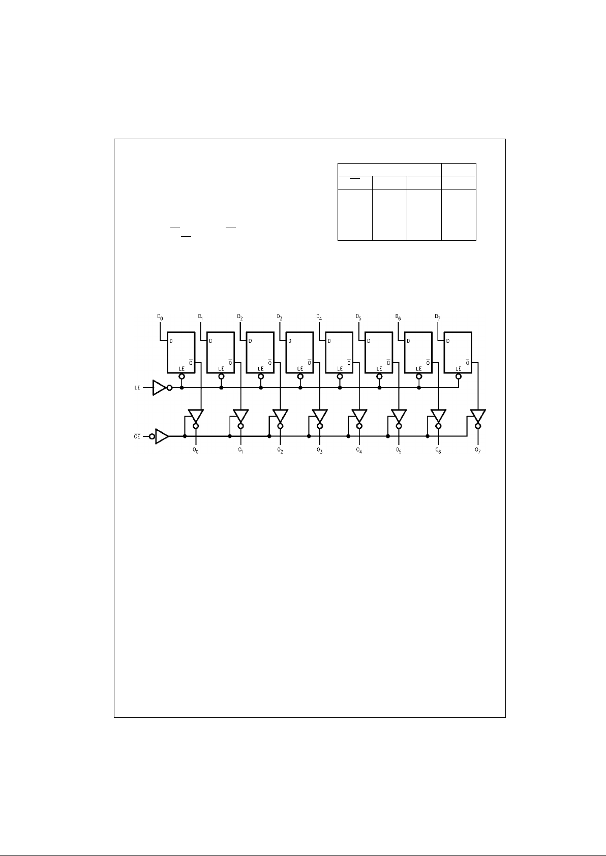
Functional Description
The VHCT573A contains eight D-type latches with 3STATE output buffers. When the Latch Enable (LE) input is
HIGH, data on the D
n
inputs enters the latches. In this con-
dition the latches are transparent, i.e., a latch o utput will
change state each time its D input cha nges. When LE is
LOW the latches store the inf ormati on th at was pres ent on
the D inputs, a setup time preceding the HIGH-to-LOW
transition of LE. The 3-STATE buffers are controlled by the
Output Enable (OE
) input. When OE is LOW, the buffers
are enabled. When OE
is HIGH the b uffers a re in the hig h
impedance mode, but, this doe s not interfere wi th entering
new data into the latches.
Tr uth Table
H = HIGH Voltage Level
L = LOW Voltage Level
X = Immaterial
Z = High Impedance
Logic Diagram
Please note that this diagram is provided o nly f or t he understanding of lo gic operations and shou ld not be used to estimate propagation delays.
Inputs Outputs
OE
LE D O
n
LHHH
LHLL
LLXO
0
HXXZ
3 www.fairchildsemi.com
74VHCT573A
Absolute Maximum Ratings(Note 2) Recommended Operating
Conditions
(Note 6)
Note 2: Absolute Maximum Ratings are valu es beyond whic h the device
may be damaged or ha ve its useful life impaire d. The datab ook specifications should be met, without exception, to ensure that the system design is
reliable over its p ower supp ly, temperature, and o utput/input loading variables. Fairchild does not recommend operation outside databook specifications.
Note 3: HIGH or LOW state. I
OUT
absolute maximum rating must be
observed.
Note 4: When outputs are in OFF-S ta t e or w hen V
CC
= OV.
Note 5: V
OUT
< GND, V
OUT
> VCC (Outputs Active).
Note 6: Unused inputs must be held HIGH or LOW. They may not float.
DC Electrical Characteristics
Noise Characteristics
Note 7: Parameter gu aranteed by design.
Supply Voltage (VCC) −0.5V to +7.0V
DC Input Voltage (V
IN
) −0.5V to +7.0V
DC Output Voltage (V
OUT
)
(Note 3) −0.5V to V
CC
+ 0.5V
(Note 4) −0.5V to +7.0V
Input Diode Current (I
IK
) −20 mA
Output Diode Current (I
OK
) (Note 5) ±20 mA
DC Output Current (I
OUT
) ±25 mA
DC V
CC
/GND Current (ICC) ±75 mA
Storage Temperature (T
STG
) −65°C to +150°C
Lead Temperature (T
L
)
(Soldering, 10 seconds) 260°C
Supply Voltage (V
CC
)4.5V to +5.5V
Input Voltage (V
IN
)0V to +5.5V
Output Voltage (V
OUT
)
(Note 3) 0V to V
CC
(Note 4) 0V to 5.5V
Operating Temperature (T
OPR
) −40°C to +85°C
Input Rise and Fall Time (t
r
, tf)
V
CC
= 5.0V ± 0.5V 0 ns/V ∼ 20 ns/V
Symbol Parameter
VCC
(V)
TA = 25°CT
A
= −40°C to +85°C
Units Conditions
Min Typ Max Min Max
V
IH
HIGH Level 4.5 2.0 2.0
V
Input Voltage 5.5 2.0 2.0
V
IL
LOW Level 4.5 0.8 0.8
V
Input Voltage 5.5 0.8 0.8
V
OH
HIGH Level 4.5 4.40 4.50 4.40 V VIN = VIHIOH = −50 µA
Output Voltage 4.5 3.94 3.80 V or VILIOH = −8 mA
V
OL
LOW Level 4.5 0.0 0.1 0.1 V VIN = VIHIOL = 50 µA
Output Voltage 4.5 0.36 0.44 V or VILIOL = 8 mA
I
OZ
3-STATE Output
5.5 ±0.25 ±2.5 µA
VIN = VIH or V
IL
Off-State Current V
OUT
= VCC or GND
I
IN
Input Leakage Current 0 − 5.5 ±0.1 ±1.0 µAVIN = 5.5V or GND
I
CC
Quiescent Supply Current 5.5 4.0 40.0 µAVIN = VCC or GND
I
CCT
Maximum ICC/Input
5.5 1.35 1.50 mA
VIN = 3.4V
Other Inputs = VCC or GND
I
OFF
Output Leakage Current
0.0 0.5 5.0 µA
V
OUT
= 5.5V
(Power Down State)
Symbol Parameter
V
CC
(V)
TA = 25°C
Units Conditions
Typ Limits
V
OLP
Quiet Output Maximum Dynamic V
OL
5.0 1.2 1.6 V CL = 50 pF
(Note 7)
V
OLV
Quiet Output Minimum Dynamic V
OL
5.0 −1.2 −1.6 V CL = 50 pF
(Note 7)
V
IHD
Minimum HIGH Level Dynamic Input Voltage 5.0 2.0 V CL = 50 pF
(Note 7)
V
ILD
Maximum LOW Level Dynamic Input Voltage 5.0 0.8 V CL = 50 pF
(Note 7)
 Loading...