

Fairchild Semiconductor 74VHCT540ASJX, 74VHCT540ASJ, 74VHCT540AN, 74VHCT540AMX, 74VHCT540AMTCX Datasheet
...
June 1997
Revised April 1999
74VHCT540A Octal Buffer/Line Driver with 3-STATE Outputs
© 1999 Fairchild Semiconductor Corporation DS500012.prf www.fairchildsemi.com
74VHCT540A
Octal Buffer/Line Driver with 3-ST ATE Outputs
General Description
The VHCT540A is an advanced high-speed CMOS device
fabricated with silicon gate CMOS technology. It achieves
the high-speed operation similar to equivalent Bipolar
Schottky TTL while maintaining the CMOS low power dissipation.
The VHCT540A is an octal buffer/line driver designed to be
employed as memory a nd address drivers, clock drivers
and bus oriented transmitter/receivers.
This device is similar in function to the VHCT240A while
providing flow-through architecture (inputs on opposite side
from outputs). This pinout ar rangement makes this de vice
especially useful as an output port for microprocessors,
allowing ease of layout and greater PC board density.
Protection circuits en sure that 0V to 7V can be applied to
the input and o utput (Note 1) pins withou t regard to the
supply voltage. This devi ce can be use d to interfa ce 3V to
5V systems and two supply systems such as battery
backup. Thi s ci r c ui t pr ev ent s d e vi ce d est r uc ti o n du e to m is matched supply and input voltages.
Note 1: Outputs in OFF-STATE
Features
■ High Speed: tPD = 5.4 ns (typ) at VCC = 5V
■ Low Power Dissipation: I
CC
= 4 µA (max) at TA = 25°C
■ Power down protection is provided on all inputs and
outputs
■ Pin and function compatible with 74HCT540
Ordering Code:
Surface mount pack ages are also available on Tape and Reel. Specify by appending the s uffix let te r “X” to the ordering code.
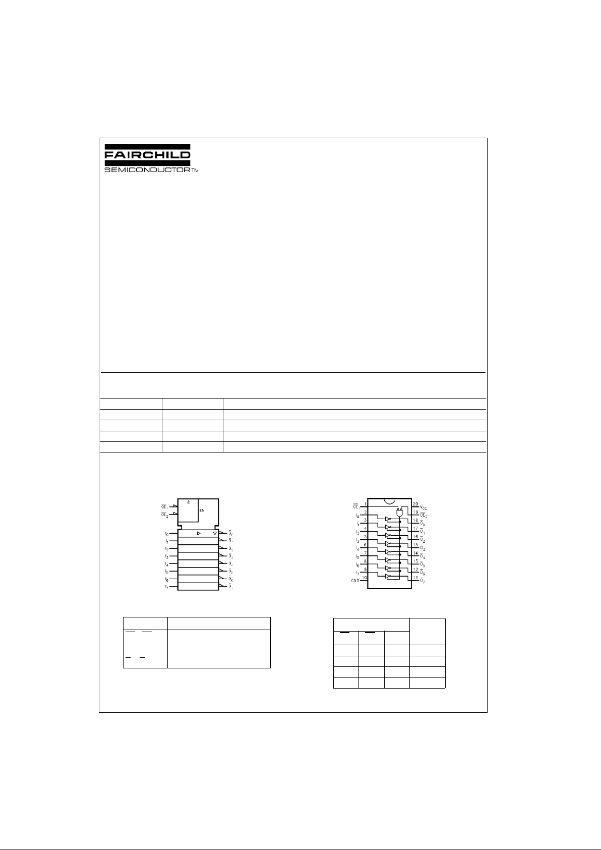
Logic Symbol
IEEE/IEC
Pin Descriptions
Connection Diagram
Truth Table
H = HIGH Voltage Level X = Immaterial
L = LOW Voltage Level Z = High Impedance
Order Number Package Number Package Dissipation
74VHCT540AM M20B 20-Lead Small Outline Integrated Circuit (SOIC), JEDEC MS-013, 0.300 Wide
74VHCT540ASJ M20D 20-Lead Small Outline Package (SOP), EIAJ TYPE II, 5.3mm Wide
74VHCT540AMTC MTC20 20-Lead Thin Shrink Small Outline Package (TSSOP), JEDEC MO-153, 4.4mm Wide
74VHCT540AN N20A 20-Lead Plastic Dual-In-Line Package (PDIP), JEDEC MS-001, 0.300 Wide
Pin Names Description
OE
1
, OE23-STATE Output Enable Inputs
I
0
- I
7
Inputs
O
0
- O
7
3-STATE Outputs
Inputs
Outputs
OE
1
OE
2
I
LLH L
HXX Z
XHX Z
LLL H
www.fairchildsemi.com 2
74VHCT540A
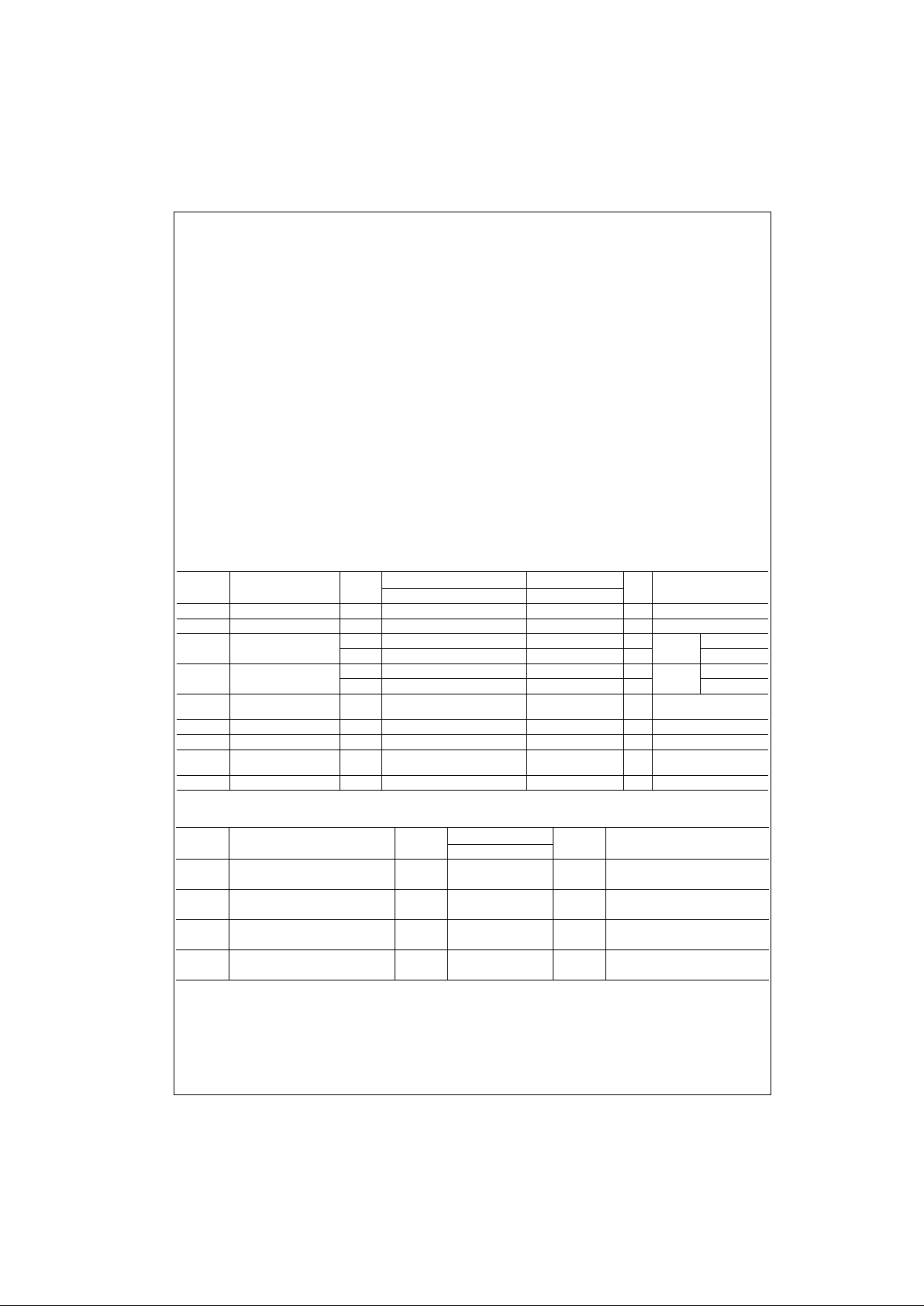
Absolute Maximum Ratings(Note 2) Recommended Operating
Conditions
(Note 6)
Note 2: Absolute Maximum Ratings are values beyond which the device
may be damaged or ha ve its useful li fe impaire d. The datab ook specifications should be met, without exception, to ensure that the system design is
reliable over its p ower supp ly, temperature, and ou tput/input loading variables. Fairchild does not recom mend operation outside data book specifications.
Note 3: When outputs are in OFF-STATE or when V
CC
= OV.
Note 4: HIGH or LOW state. I
OUT
absolute maximum rating must be
observed.
Note 5: V
OUT
<GND, V
OUT
> V
CC (outputs active).
Note 6: Unused inputs must be held HIGH or LOW. They may not float.
DC Electrical Characteristics
Noise Characteristics
Note 7: Paramete r guaranteed by design.
Supply Voltage (VCC) −0.5V to +7.0V
DC Input Voltage (V
IN
) −0.5V to +7.0V
DC Output Voltage (V
OUT
)
(Note 3) −0.5V to +7.0V
(Note 4) −0.5V to V
CC
+ 0.5V
Input Diode Current (I
IK
) −20 mA
Output Diode Current (I
OK
)
(Note 5) ±20 mA
DC Output Current (I
OUT
) ±25 mA
DC V
CC
/GND Current (ICC) ±75 mA
Storage Temperature (T
STG
) −65°C to +150°C
Lead Temperature (T
L
)
(Soldering, 10 seconds) 260°C
Supply Voltage (V
CC
) 4.5V to +5.5V
Input Voltage (V
IN
)0V to +5.5V
Output Voltage (V
OUT
)
(Note 4) 0V to V
CC
(Note 3) 0V to 5.5V
Operating Temperature (T
OPR
) −40°C to +85°C
Input Rise and Fall Time (t
r
, tf)
V
CC
= 5.0V ± 0.5V 0 ≈ 20 ns/V
Symbol Parameter
V
CC
(V)
TA = 25°CT
A
= −40°C to +85°C
Units Conditions
Min Typ Max Min Max
V
IH
HIGH Level Input Voltage 4.5 − 5.5 2.0 2.0 V
V
IL
LOW Level Input Voltage 4.5 − 5.5 0.8 0.8 V
V
OH
HIGH Level 4.5 4.4 4.5 4.4 V VIN = VIH IOH = −50 µA
Output Voltage 4.5 3.94 3.80 V or VILIOH = −8 mA
V
OL
LOW Level 4.5 0.0 0.1 0.1 V VIN = VIH IOL = 50 µA
Output Voltage 4.5 0.36 0.44 V or VILIOL = 8 mA
I
OZ
3-STATE Output
OFF-STATE Current
5.5 ±0.25 ±2.5 µA
VIN = VIH or V
IL
V
OUT
= VCC or GND
I
IN
Input Leakage Current 0 − 5.5 ±0.1 ±1.0 µAVIN = 5.5V or GND
I
CC
Quiescent Supply Current 5.5 4.0 40.0 µAVIN = VCC or GND
I
CCT
Maximum I
CC/input
5.5 1.35 1.50 mA
VIN = 3.4V
other in puts = VCC or GND
I
OFF
Output Leakage Current 0 0.5 5.0 µAV
OUT
= 5.5V
Symbol Parameter
VCC
(V)
TA = 25°C
Units Conditions
Typ Limits
V
OLP
Quiet Output Maximum
5.0 1.2 1.6 V CL = 50 pF
(Note 7) Dynamic V
OL
V
OLV
Quiet Output Minimum
5.0 −1.2 1.6 V CL = 50 pF
(Note 7) Dynamic V
OL
V
IHD
Minimum HIGH Level Dynamic
5.0 2.0 V CL = 50 pF
(Note 7) Input Voltage
V
ILD
Maximum HIGH Level Dynamic
5.0 0.8 V CL = 50 pF
(Note 7) Input Voltage
 Loading...