Fairchild Semiconductor 74LVX112SJX, 74LVX112SJ, 74LVX112MX, 74LVX112MTCX, 74LVX112MTC Datasheet
...
October 1996
Revised March 1999
74LVX112 Low Voltage Dual J-K Flip-Flops with Preset and Clear
© 1999 Fairchild Semiconductor Corporation DS012158.prf www.fairchildsemi.com
74LVX112
Low Voltage Dual J-K Flip-Flops with Preset and Clear
General Description
The LVX112 is a dual J-K Flip-Flop where each flip-flop has
independent inputs (J, K, PRESET, CLEAR, and CLOCK)
and outputs (Q, Q
). These devices are edge sen sitive and
change states synchronou sly on th e neg ative go ing transition of the clock pu lse. Triggering o ccurs a t a voltag e l evel
of the clock and is not directly related to the transition time.
Clear and Preset are independent of the clock and are
accomplished by a low logic level on the corresponding
input. The J and K inpu ts can change w hen the clo ck is in
either state without affecting the flip-flop, provided that they
are in the desired state during the recommended setup and
hold times relative to the falling edge of the clock.
The inputs tolerate voltages up to 7V allowing the interface
of 5V systems to 3V systems.
Features
■ Input voltage level translation from 5V–3V
■ Ideal for low power/low noise 3.3V applications
Ordering Code:
Devices also availab le in Tape and Reel. Specify by appending su ffix let te r “X” to the ordering code.
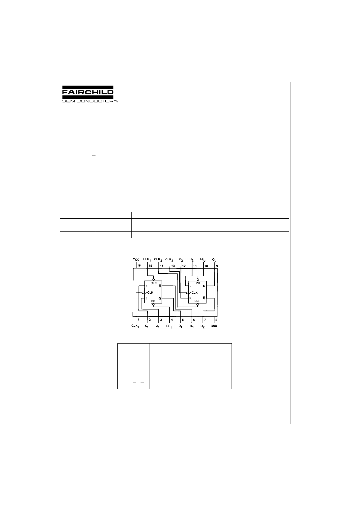
Connection Diagram
Pin Descriptions
Order Number Package Number Package Description
74LVX112M M16A 16-Lead Small Outline Integrated Circuit (SOIC), JEDEC MS-012, 0.150” Narrow
74LVX112SJ M16D 16-Lead Small Outline Package (SOP), EIAJ TYPE II, 5.3mm Wide
74LVX112MTC MTC16 16-Lead Thin Shrink Small Outline Package (TSSOP), JEDEC MO-153, 4.4mm Wide
Pin Names Description
J
1
, J2, K1, K2Data Inputs
CLK
1
, CLK2Clock Pulse Inputs (Active Falling edge)
CLR
1
, CLR2Direct Clear Inputs (Active LOW)
PR
1
, PR
2
Direct Preset Inputs (Active LOW)
Q
1
, Q2, Q1, Q
2

www.fairchildsemi.com 2
74LVX112
Truth Table
H (h) = HIGH Voltage Level
L (l) = LOW Voltage Level
X = Immaterial
= HIGH-to-LOW C loc k Transit ion
Q
0
(Q0) = Before HIGH-to-LOW Transition of Clock
Lower case letters indicate the state of the ref erenced input or ou tp ut one setup time prior to the H I GH-to-LOW clock tra ns it io n.
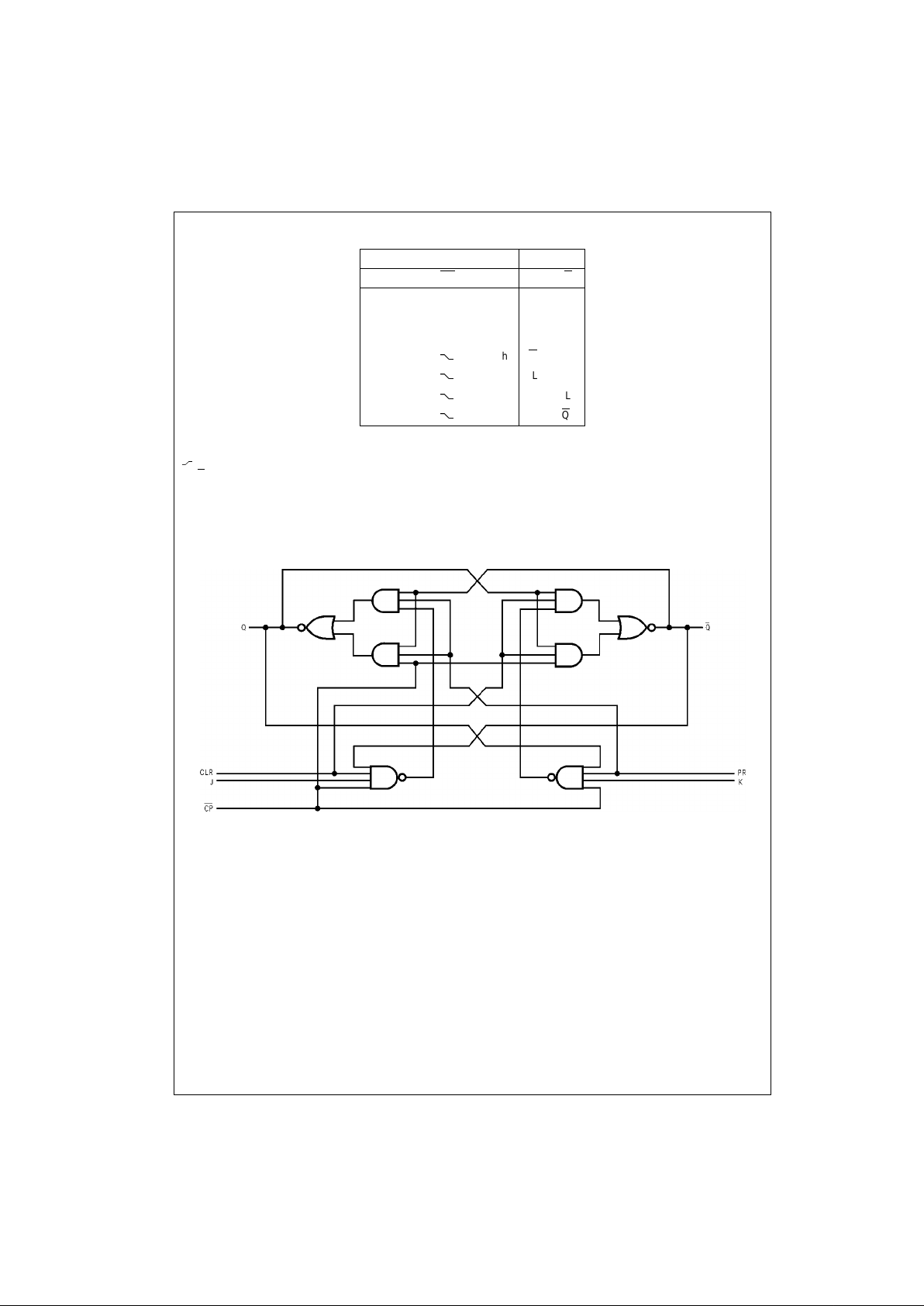
Logic Diagram
(One Half Shown)
Inputs Outputs
PR CLR CP
JKQ Q
LHXXXHL
HLXXXLH
LLXXXHH
HH
hhQ0Q
0
HH
lhL H
HH
hlH L
HH
llQ0Q
0
 Loading...