© 1999 Fairchild Semiconductor Corporation DS009488 www.fairchildsemi.com
April 1988
Revised July 1999
74F169 4-Stage Synchronous Bidirectional Counter
74F169
4-Stage Synchronous Bidirectional Counter
General Description
The 74F169 is a fully synchronous 4-stage up/down
counter. The 74F169 is a modulo- 16 binary counter. Features a preset capability for programmable operation, carry
lookahead for easy cascad ing and a U/D
input to control
the direction of counting. All state changes, whether in
counting or parallel load ing, are initiated by the LOW-toHIGH transition of the clock.
Features
■ Asynchro nous counting and loading
■ Built-in lookahead carry capability
■ Presettable for programmable operation
Ordering Code:
Devices also availab le in Tape and Reel. Specify by appending th e s uffix let t er “X” to the ordering code.
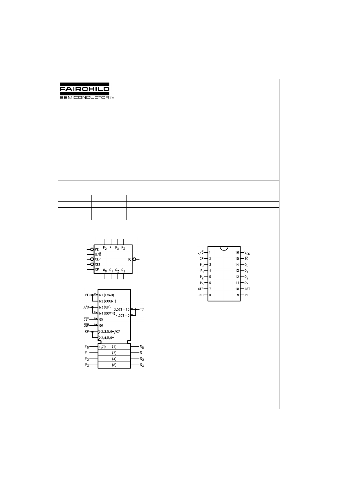
Logic Symbols
IEEE/IEC
Connection Diagram
Order Number Package Number Package Description
74F169SC M16A 16-Lead Small Outline Integrated Circuit (SOIC), JEDEC MS-012, 0.150 Narrow
74F169SJ M16D 16-Lead Small Outline Package (SOP), EIAJ TYPE II, 5.3mm Wide
74F169PC N16E 16-Lead Plastic Dual-In-Line Package (PDIP), JEDEC MS-001, 0.300 Wide

www.fairchildsemi.com 2
74F169
Unit Loading/Fan Out
Functional Description
The 74F169 uses edge-triggered J-K type flip-flops and
has no constraints on changing the control or data input
signals in either stat e of the c lock. The only req uireme nt is
that the various inpu ts attain the desired state at least a
setup time before the rising edge of the clock and rema in
valid for the recom mend ed hold time therea fter. The parallel load operation t akes prece dence o ver ot her op eration s,
as indicated in the Mode Select Table. When PE
is LOW,
the data on the P
0–P3
inputs enters the flip-flops on the
next rising edge of the clock. In order for counting to occur,
both CEP
and CET must be LOW an d PE must be HI GH;
the U/D
input then determines the direction of counting.
The Terminal C o unt ( TC
) output is normally HIGH and goes
LOW, provided that CET
is LOW, when a counter reach es
zero in the Count Down mode or reaches 15 for the
74F169 in the Count Up mode. The TC
output state is not a
function of the Count Enable Parallel (CEP
) input level.
Since the TC
signal is derived by decoding the flip-flop
states, there exists the p ossibility of decoding spikes on
TC
. For this reason the use of T C as a clock signal is not
recommended (see logic equations below).
1. Count Enable = CEP
• CET • PE
2. Up: (74F169): TC = Q0 • Q1 • Q2 • Q3 • (Up) • CET
3. Down: TC = Q0 • Q1 • Q2 • Q3 • (Down) • CET
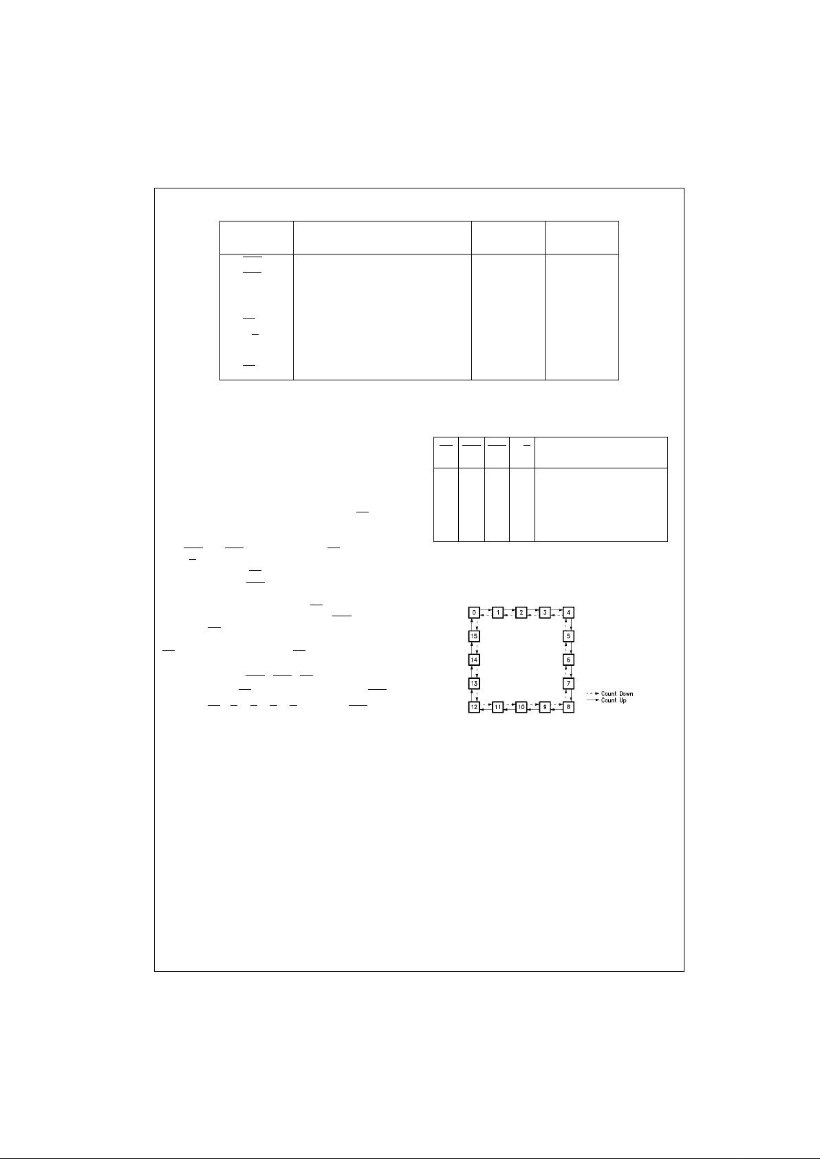
Mode Select Table
H = HIGH Voltage Level
L = LOW Voltage Level
X = Immaterial
State Diagram
Pin Names Description
U.L.
Input I
IH/IIL
HIGH/LOW
Output I
OH/IOL
CEP
Count Enable Parallel Input (Active LOW) 1.0/1.0 20 µA/−0.6 mA
CET
Count Enable Trickle Input (Active LOW) 1.0/2.0 20 µA/−1.2 mA
CP Clock Pulse Input (Active Rising Edge) 1.0/1.0 20 µA/−0.6 mA
P
0–P3
Parallel Data Inputs 1.0/1.0 20 µA/−0.6 mA
PE
Parallel Enable Input (Active LOW) 1.0/1.0 20 µA/−0.6 mA
U/D
Up-Down Count Control Input 1.0/1.0 20 µA/−0.6 mA
Q
0–Q3
Flip-Flop Outputs 50/33.3 −1 mA/20 mA
TC
Terminal Count Output (Active LOW) 50/33.3 −1 mA/20 mA
PE CEP CET U/D
Action on Rising
Clock Edge
L X X X Load (P
n
→ Qn)
H L L H Count Up (Increment)
H L L L Count Down (Decrement)
H H X X No Change (Hold)
H X H X No Change (Hold)

3 www.fairchildsemi.com
74F169
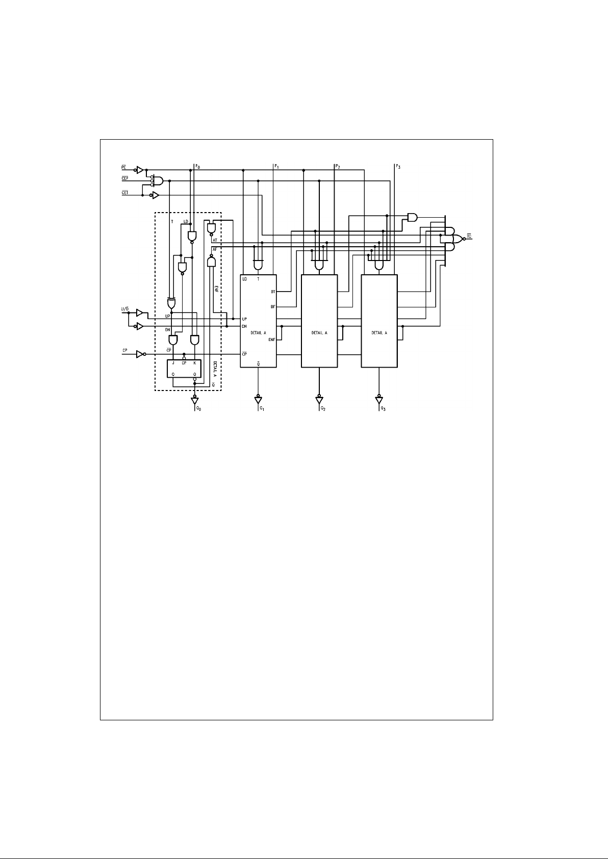
Logic Diagram
Please note that thes e diagrams are provide d only for the understan ding of logic operations a nd should not be used to es t im ate propagation delays.
 Loading...