Fairchild Semiconductor 74F164ASJX, 74F164ASJ, 74F164ASCX, 74F164ASC, 74F164APC Datasheet
...
© 1999 Fairchild Semiconductor Corporation DS010613 www.fairchildsemi.com
October 1989
Revised August 1999
74F164A Serial-In, Parallel-Out Shift Register
74F164A
Serial-In, Parallel-Out Shift Register
General Description
The 74F164A is a high-speed 8-bit serial-in/parallel-out
shift register. Serial data is entered thr ough a 2-in put AND
gate synchronous wit h the LOW-to-HIGH transition of the
clock. The device features an asynchron ous Master Re set
which clears the registe r, setting all output s LOW inde pendent of the clock. The 74F16 4A is a faster version of the
74F164.
Features
■ Typical shift frequency of 90 MHz
■ Asynchronous Master Reset
■ Gated serial data input
■ Fully synchronous data transfers
■ 74F164A is a faster version of the 74F164
Ordering Code:
Devices also availab le in Tape and Reel. Specify by appending th e s uffix let t er “X” to the ordering code.
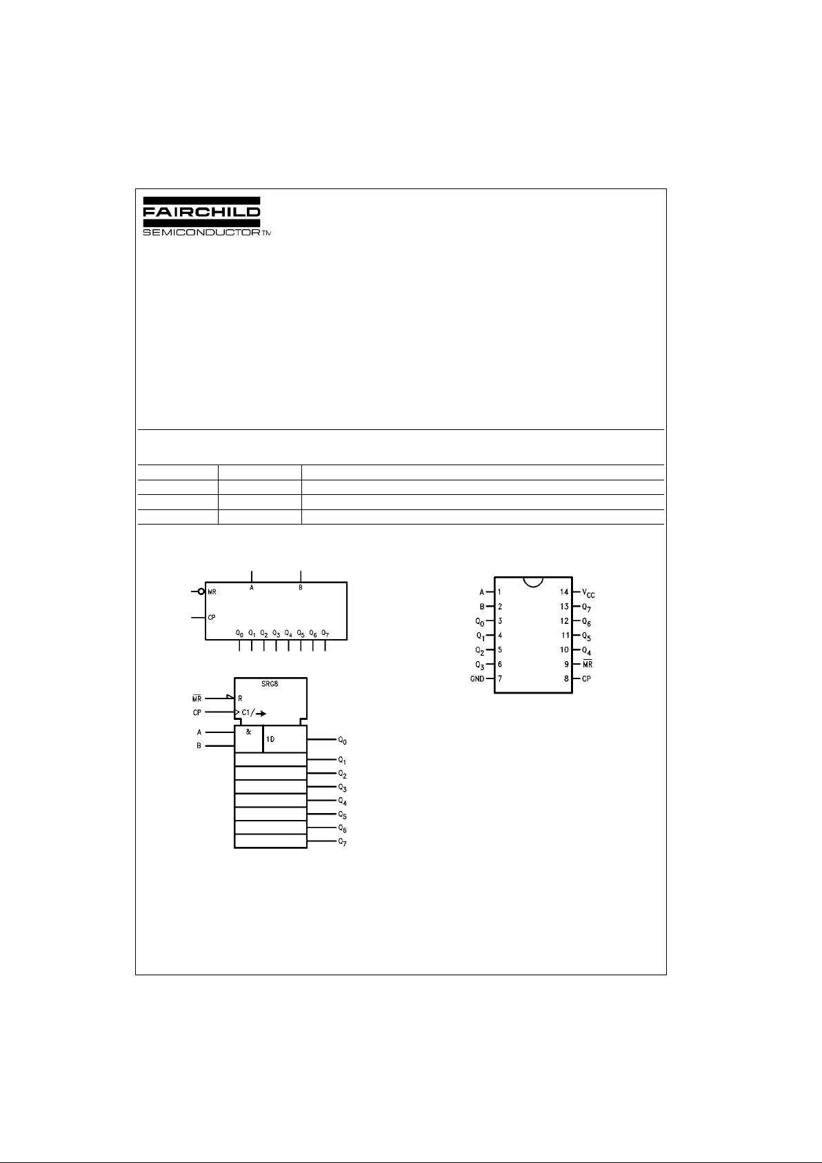
Logic Symbols
IEEE/IEC
Connection Diagram
Order Number Package Number Package Description
74F164ASC M14A 14-Lead Small Outline Integrated Circuit (SOIC), JEDEC MS-120, 0.150 Narrow
74F164ASJ M14D 14-Lead Small Outline Package (SOP), EIAJ TYPE II, 5.3mm Wide
74F164APC N14A 14-Lead Plastic Dual-In-Line Package (PDIP), JEDEC MS-001, 0.300 Wide

www.fairchildsemi.com 2
74F164A
Unit Loading/Fan Out
Functional Description
The 74F164A is a n edge-triggered 8- bit shift register with
serial data entry and an output from each of the eight
stages. Data is entere d serially through one of tw o inputs
(A or B); either of t hese inputs can be used as a n active
HIGH Enable for da ta entry through the other input. An
unused input must be tied HIGH.
Each LOW-to-HIGH transition on the Clock (CP) input
shifts data one place to the right and enters into Q
0
the log-
ical AND of the two data inputs (A • B) that existed before
the rising clock edg e. A LOW level on the Master Reset
(MR
) input overrides all other inputs and clears the register
asynchronously, forcing all Q outputs LOW.
Mode Select Table
H(h) = HIGH Voltage Levels
L(l) = LOW Voltage Levels
X = Immaterial
q
n
= Lower case le tters indi cate the s tate of the referenc ed input or outpu t
one setup time prior to t he LOW-to-HIGH clock tr ansition.
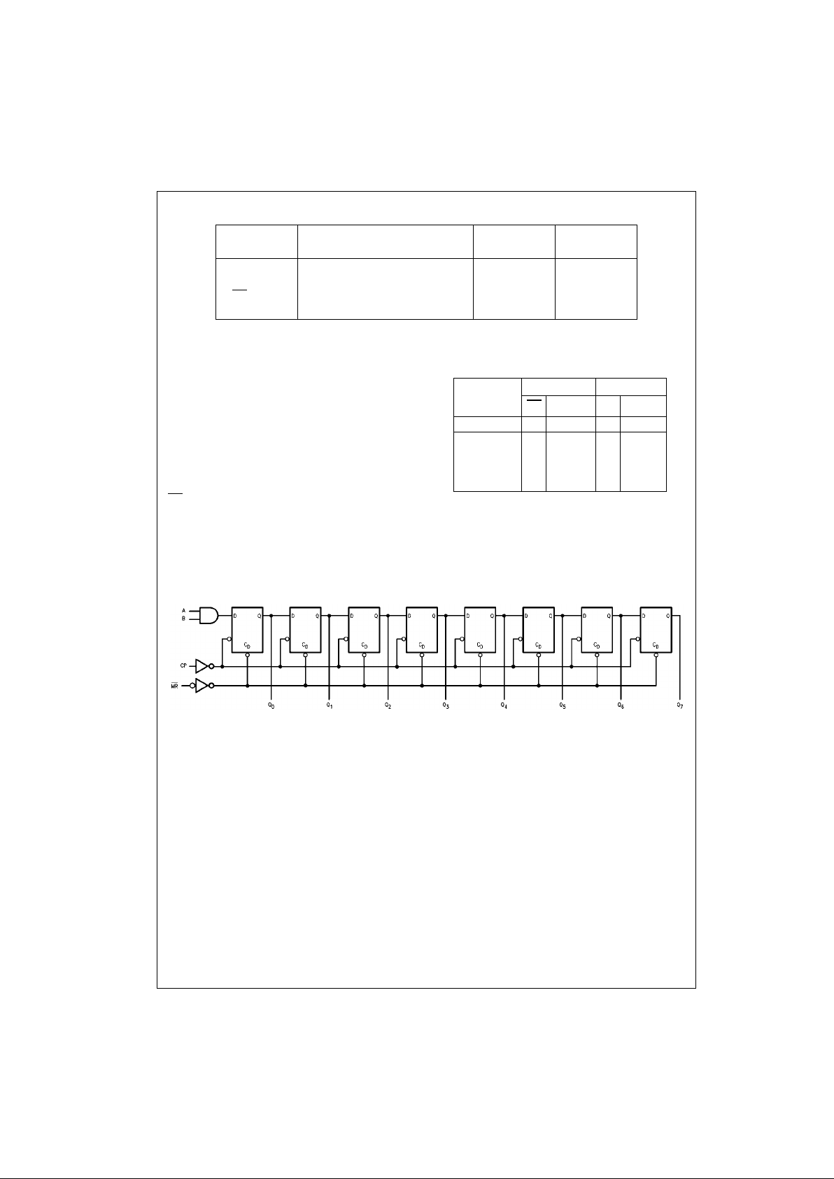
Logic Diagram
Please note that this diagram is provided o nly f or t he understanding of lo gic operations and should not be used to estimate propagation delays.
Pin Names Description
U.L.
Input I
IH/IIL
HIGH/LOW
Output I
OH/IOL
A, B Data Inputs 1.0/1.0 20 µA/−0.6 mA
CP Clock Pulse Input (Active Rising Edge) 1.0/1.0 20 µA/−0.6 mA
MR
Master Reset Input (Active LOW) 1.0/1.0 20 µA/−0.6 mA
Q
0–Q7
Outputs 50/33.3 −1 mA/20 mA
Operating Inputs Outputs
Mode MR
AB
Q
0Q1–Q7
Reset (Clear) L X X L L-L
Hl lLq
0–q6
Shift H l h L q0–q
6
Hh l Lq0–q
6
HhhHq0–q
6
 Loading...