

Fairchild Semiconductor 74ALVC16821 Datasheet
74ALVC16821
Low Voltage 20-Bit D-Type Flip-Flops
with 3.6V Tolerant Inputs and Outputs
74ALVC16821 Low Voltage 20-Bit D-Type Flip-Flops with 3.6V Tolerant Inputs and Outputs
October 2001
Revised October 2001
General Description
The ALVC16821 contains twenty non-inverting D-type
flip-flops with 3-STATE outputs and is intended for bus oriented applications.
The 74ALVC16821 is designed for low voltage (1.65V to
3.6V) V
The 74ALVC16821 is fabricated w ith an advanc ed CMOS
technology to achieve high speed operation while maintaining low CMOS power dissipation.
applications with I/O compatibility up to 3.6V.
CC
Features
■ 1.65V–3.6V VCC supply operation
■ 3.6V tolerant inputs and outputs
■ t
PD
4.0 ns max for 3.0V to 3.6V V
4.9 ns max for 2.3V to 2.7V V
8.8 ns max for 1.65V to 1.95V V
■ Power-off high impedance inputs and outputs
■ Supports live insertion and withdrawal (Note 1)
■ Uses patented noise/EMI reductio n circuitr y
■ Latchup conforms to JEDEC JED78
■ ESD performance:
Human body model
Machine model
Note 1: To ensure the high-impedance state d uring power up or power
down, OE
should be tied to VCC through a pull-up r esistor; the min imum
value of the res istor is d eter mine d by the cu rre nt-sou rcin g ca pa bility of t he
driver.
> 200V
CC
CC
CC
> 2000V
Ordering Code:
Order Number Package Number Package Descriptions
74ALVC16821MTD MTD56 56-Lead Thin Shrink Small Outline Package (TSSOP), JEDEC MO-153, 6.1mm Wide
Device also available in Tape and Reel. Specify by appending suffix letter “X” to the ordering co de.
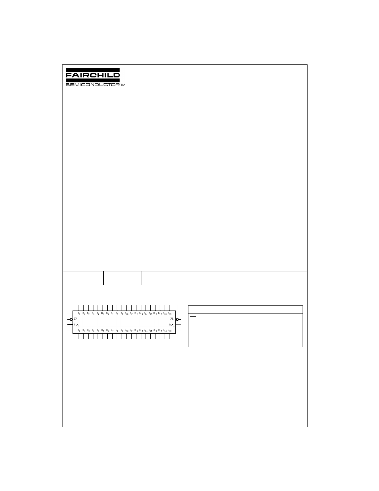
Logic Symbol Pin Descriptions
Pin Names Description
OE
CLK
D
0–D19
O
0–O19
n
n
Output Enable Input (Active LOW)
Clock Input
Inputs
Outputs
© 2001 Fairchild Semiconductor Corporation DS500685 www.fairchildsemi.com
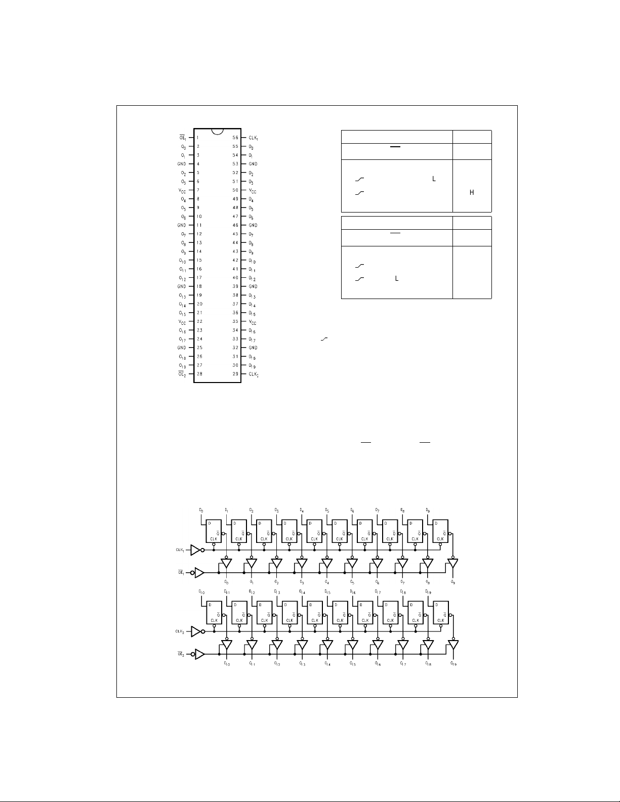
Connection Diagram Truth Tables
CLK
74ALVC16821
L or H L X O
CLK
L or H L X O
H = HIGH Voltage Level
L = LOW Voltage Level
X = Immaterial (HIGH or LOW, inputs may not float)
Z = High Impedance
= Previous O0 before L O W-to-HIGH tran sition of Clock
O
0
= LOW-to-HIGH transition
Functional Description
The 74ALVC16821 contains twenty D-type flip-fl ops with
3-STATE standard outputs. The device is byte control led
with each byte functioning ide ntically, but independent of
each other. Control pins can be shorted together to obtain
full 20-bit operation. The following description applies to
each byte. The twenty flip- flops will store the state of their
individual D-type inputs that meet the setup and hold time
requirements on th e LOW-to-H IGH Clock (CLK) trans ition.
The 3-STATE standard outputs are controlled by the O utput Enable (OE
outputs are in th e high i mpedan ce mode but this does not
interfere with entering new data into the flip-flops.
Inputs Outputs
OE
1
D0–D
1
O0–O
9
9
XHXZ
LLL
LHH
0
Inputs Outputs
OE
2
D10–D19O10–O
2
19
XHXZ
LLL
LHH
0
) input. When OEn is HIGH, the standard
n
Logic Diagrams
Please note that this diagram is provided only for the understanding of logic operations and should not be used to estimate propagation delays.
www.fairchildsemi.com 2
 Loading...